
List of Semiconductor Manufacturing Equipment products
- classification:Semiconductor Manufacturing Equipment
1~45 item / All 5250 items


It won't break even after 1 million repetitions! A mat switch with reliable operation, high durability, and low price. Suitable for options in machine tools as well. Please consult us about delivery t...
- Sensors


We can accommodate high resistance over 10,000 ohms, with diameters ranging from approximately 30 mm to 8 inches, and we also offer thinning and chip processing arrangements!
- Other semiconductors
- Processing Contract
- Wafer


Visualize surface foreign substances, dirt, and scratches! It is well-received as a daily management tool for yield management, quality control, cleaning management, and hygiene management. *Demo unit...
- Visual Inspection Equipment
- Semiconductor inspection/test equipment
- Defect Inspection Equipment
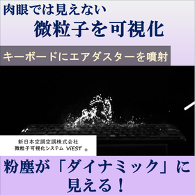
17th High-Performance Materials WEEK [Tokyo] We will be exhibiting a fine particle visualization system at the 17th High-Performance Film Exhibition. (September 30, 2026 (Wed) - October 2, 2026 (Fri) / Makuhari Messe, Hall 2)
The particle visualization technology developed under our brand "ViEST" has a very high level of detection sensitivity that allows for real-time visualization of the suspended and adhered states of micro and nano-sized particles. We are expanding our sales of visualization systems and providing evaluation services (such as investigating particles and airflow in production processes, manufacturing equipment, and factory environments, evaluating the performance of cleaning products, and proposing yield improvement measures) both domestically and internationally. We consistently support the identification of causes and the formulation of countermeasures by visualizing fine foreign substances, particle adhesion due to static electricity, and variations in cleanliness that are problematic in the film manufacturing process. The following are some examples of applications, but by utilizing our technology, we can strongly promote the resolution of various issues such as the deterioration of defect rates caused by fine foreign substances, visualization of clean airflow, and concerns regarding site cleanliness. - Visualization of foreign matter contamination and adhesion mechanisms in the coating and drying processes - Visualization of dust generation and re-adhesion during roll transportation and consideration of countermeasures - Evaluation of airflow and cleanliness within clean booths/clean rooms - Identification of dust sources within manufacturing equipment and promotion of cleanliness - Reduction of foreign matter adhesion risk on film surfaces and improvement of yield
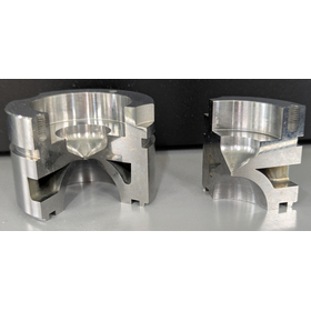

We meet the high precision needs of semiconductor manufacturing with microfabrication and diffusion bonding.
- Special Processing Machinery
- Heat exchanger
- Oxidation/Diffusion Device
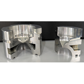
We expand possibilities with microfabrication and diffusion bonding.
- Special Processing Machinery
- Oxidation/Diffusion Device
- Heat exchanger

Joining different materials without melting: A joining technology that balances precision and strength.
- Welding Machine
- Oxidation/Diffusion Device
- Processing Contract
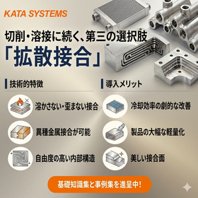
Please use it for demonstration tests and research and development.
- Processing Contract
- Contract manufacturing
- Semiconductor inspection/test equipment


We are a manufacturer specializing in filter housings.
- Other semiconductor manufacturing equipment
- Other filters
- Filtration Equipment

It is a manufacturer specializing in filter housings.
- Other semiconductor manufacturing equipment
- Other filters
- Filtration Equipment

We are a manufacturer specializing in filter housings.
- Other semiconductor manufacturing equipment
- Other filters
- Filtration Equipment

We are a manufacturer specializing in filter housings.
- Other semiconductor manufacturing equipment
- Other filters
- Filtration Equipment

We are a manufacturer specializing in filter housings.
- Other semiconductor manufacturing equipment

It is a manufacturer specializing in filter housings.
- Other semiconductor manufacturing equipment
- Beverage Production Equipment
- Filtration Equipment

It excels in high sensitivity detection, quantification, and portability, making it suitable for quality inspection and research and development settings. It contributes to the detection of minute for...
- Semiconductor inspection/test equipment
- Other Sanitation Inspections
- Other appearance and image inspection equipment
17th High-Performance Materials WEEK [Tokyo] We will be exhibiting a fine particle visualization system at the 17th High-Performance Film Exhibition. (September 30, 2026 (Wed) - October 2, 2026 (Fri) / Makuhari Messe, Hall 2)
The particle visualization technology developed under our brand "ViEST" has a very high level of detection sensitivity that allows for real-time visualization of the suspended and adhered states of micro and nano-sized particles. We are expanding our sales of visualization systems and providing evaluation services (such as investigating particles and airflow in production processes, manufacturing equipment, and factory environments, evaluating the performance of cleaning products, and proposing yield improvement measures) both domestically and internationally. We consistently support the identification of causes and the formulation of countermeasures by visualizing fine foreign substances, particle adhesion due to static electricity, and variations in cleanliness that are problematic in the film manufacturing process. The following are some examples of applications, but by utilizing our technology, we can strongly promote the resolution of various issues such as the deterioration of defect rates caused by fine foreign substances, visualization of clean airflow, and concerns regarding site cleanliness. - Visualization of foreign matter contamination and adhesion mechanisms in the coating and drying processes - Visualization of dust generation and re-adhesion during roll transportation and consideration of countermeasures - Evaluation of airflow and cleanliness within clean booths/clean rooms - Identification of dust sources within manufacturing equipment and promotion of cleanliness - Reduction of foreign matter adhesion risk on film surfaces and improvement of yield


Atomization of liquid without pressurization by piezo vibration. Enables uniform application while reducing power consumption and liquid waste.


- spray
- Coating Machine
- CMP Equipment
Start of distribution of 3D CAD data for Sonia Corporation's ultrasonic spray nozzle.
We have started distributing 3D CAD data for the Sonia ultrasonic spray nozzles. Designers and equipment manufacturers can efficiently proceed with equipment design and layout considerations by confirming product shapes and mounting dimensions in advance. This time, we have also released the 3D CAD data for the ultrasonic spray nozzles "WS40K" and "WS130K," which can be used for interference checks and design simulations before implementation. Sonia's ultrasonic spray nozzles cater to a wide range of applications, including precision coating, surface treatment, humidification, and cleaning. By providing 3D CAD data, we support the reduction of design man-hours and the shortening of development periods, facilitating a smooth process from product selection to equipment development.
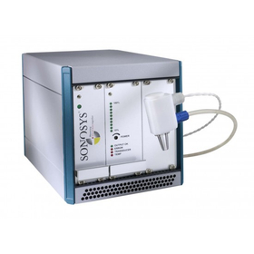
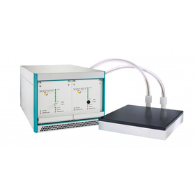
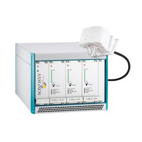
Thorough removal of fine contaminants from wafers. High-quality cleaning achieved by Sonosys.
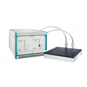
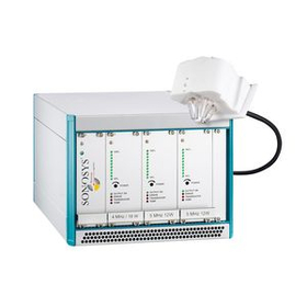
- Ultrasonic Cleaner
- Ultrasonic Oscillator
- Photomask
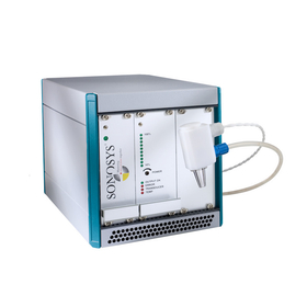
Announcement of the release of the latest leaflet for the SONOSYS Corporation's megasonic cleaning device.
We have updated the product leaflet for the SONOSYS megasonic cleaning device from Germany to the latest version. SONOSYS's megasonic cleaning technology is a non-contact precision cleaning technique that efficiently removes fine particles by transmitting high-frequency ultrasonic energy through liquids such as pure water (DI Water) to the surface of the target object. It is particularly suitable for the precision cleaning of products with fine structures, such as semiconductor wafers, photomasks, MEMS, various substrates, and optical components, and is utilized in various fields that require high cleanliness, starting with semiconductor manufacturing processes. SONOSYS offers a range of frequencies depending on the application and the particles to be removed, as well as a megasonic nozzle system that accommodates various cleaning conditions, including Single Nozzle, Dual Nozzle, and Triple Nozzle. Customers who have challenges such as "wanting to remove fine particles from wafers," "wanting to clean photomasks and MEMS while minimizing damage," or "wanting to review existing cleaning processes" are encouraged to take a look at the latest leaflet.
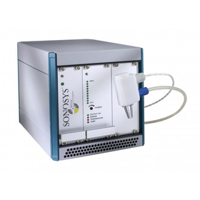
For precise cleaning of prisms. Sonosys ultrasonic cleaning device.
- Ultrasonic Cleaner
- Ultrasonic Oscillator
- Photomask
Announcement of the release of the latest leaflet for the SONOSYS Corporation's megasonic cleaning device.
We have updated the product leaflet for the SONOSYS megasonic cleaning device from Germany to the latest version. SONOSYS's megasonic cleaning technology is a non-contact precision cleaning technique that efficiently removes fine particles by transmitting high-frequency ultrasonic energy through liquids such as pure water (DI Water) to the surface of the target object. It is particularly suitable for the precision cleaning of products with fine structures, such as semiconductor wafers, photomasks, MEMS, various substrates, and optical components, and is utilized in various fields that require high cleanliness, starting with semiconductor manufacturing processes. SONOSYS offers a range of frequencies depending on the application and the particles to be removed, as well as a megasonic nozzle system that accommodates various cleaning conditions, including Single Nozzle, Dual Nozzle, and Triple Nozzle. Customers who have challenges such as "wanting to remove fine particles from wafers," "wanting to clean photomasks and MEMS while minimizing damage," or "wanting to review existing cleaning processes" are encouraged to take a look at the latest leaflet.
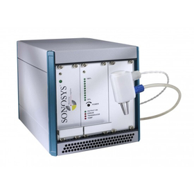
Leave the latest ultrasonic cleaning to Sonosys.


- Photomask
- CMP Equipment
- CVD Equipment
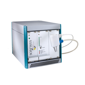
The NHK program "The Wall of Truth" will feature a video of semiconductor wafer cleaning provided by our company.
We are pleased to announce that a video provided by Tick Corporation showcasing semiconductor wafer cleaning will be featured in the NHK program "The Wall of Truth." The theme for this episode is "The Truth of Water (tentative)." The program is scheduled to briefly introduce the process of cleaning wafers with pure water during semiconductor manufacturing. Our company offers cleaning and spraying technologies, including megasonic cleaning, for the semiconductor and electronic components sectors. We are truly honored that our footage will be utilized in the production of this NHK program. Broadcast schedule: September 12, 2026 (Saturday) from 8:30 PM to 8:59 PM (tentative). For more details about the program, please visit the official NHK "The Wall of Truth" page. https://www.nhk.jp/g/ts/N8JX1V6V69/ *Please note that the broadcast date and content may be subject to change.

Flow spray of 2 mmlit/min or less is possible!
- nozzle
- valve
- Etching Equipment
Start of distribution of 3D CAD data for Sonia Corporation's ultrasonic spray nozzle.
We have started distributing 3D CAD data for the Sonia ultrasonic spray nozzles. Designers and equipment manufacturers can efficiently proceed with equipment design and layout considerations by confirming product shapes and mounting dimensions in advance. This time, we have also released the 3D CAD data for the ultrasonic spray nozzles "WS40K" and "WS130K," which can be used for interference checks and design simulations before implementation. Sonia's ultrasonic spray nozzles cater to a wide range of applications, including precision coating, surface treatment, humidification, and cleaning. By providing 3D CAD data, we support the reduction of design man-hours and the shortening of development periods, facilitating a smooth process from product selection to equipment development.

Next-generation megasonic technology can instantly clear wafers up to 300mm.
- Photomask
- Other semiconductor manufacturing equipment
- Ultrasonic Cleaner
The NHK program "The Wall of Truth" will feature a video of semiconductor wafer cleaning provided by our company.
We are pleased to announce that a video provided by Tick Corporation showcasing semiconductor wafer cleaning will be featured in the NHK program "The Wall of Truth." The theme for this episode is "The Truth of Water (tentative)." The program is scheduled to briefly introduce the process of cleaning wafers with pure water during semiconductor manufacturing. Our company offers cleaning and spraying technologies, including megasonic cleaning, for the semiconductor and electronic components sectors. We are truly honored that our footage will be utilized in the production of this NHK program. Broadcast schedule: September 12, 2026 (Saturday) from 8:30 PM to 8:59 PM (tentative). For more details about the program, please visit the official NHK "The Wall of Truth" page. https://www.nhk.jp/g/ts/N8JX1V6V69/ *Please note that the broadcast date and content may be subject to change.
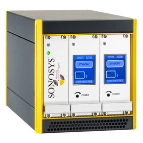
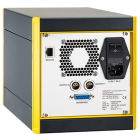
The Digital Generator is a digital control generator compatible with megasonic cleaning systems for semiconductors, electronic components, and precision instruments.
- Photomask
- Other semiconductor manufacturing equipment
- Wafer
The NHK program "The Wall of Truth" will feature a video of semiconductor wafer cleaning provided by our company.
We are pleased to announce that a video provided by Tick Corporation showcasing semiconductor wafer cleaning will be featured in the NHK program "The Wall of Truth." The theme for this episode is "The Truth of Water (tentative)." The program is scheduled to briefly introduce the process of cleaning wafers with pure water during semiconductor manufacturing. Our company offers cleaning and spraying technologies, including megasonic cleaning, for the semiconductor and electronic components sectors. We are truly honored that our footage will be utilized in the production of this NHK program. Broadcast schedule: September 12, 2026 (Saturday) from 8:30 PM to 8:59 PM (tentative). For more details about the program, please visit the official NHK "The Wall of Truth" page. https://www.nhk.jp/g/ts/N8JX1V6V69/ *Please note that the broadcast date and content may be subject to change.