
List of Semiconductor Manufacturing Equipment products
- classification:Semiconductor Manufacturing Equipment
271~315 item / All 5250 items


It won't break even after 1 million repetitions! A mat switch with reliable operation, high durability, and low price. Suitable for options in machine tools as well. Please consult us about delivery t...
- Sensors


We can accommodate high resistance over 10,000 ohms, with diameters ranging from approximately 30 mm to 8 inches, and we also offer thinning and chip processing arrangements!
- Other semiconductors
- Processing Contract
- Wafer


High-performance multi-sputtering device 6-element multi-sputter (for Φ4 inch) 4-element multi-sputter (for Φ6, 8 inch)
- Sputtering Equipment
- Evaporation Equipment
- Etching Equipment

BH Series [UHV Compatible Ultra-High Temperature Vacuum Thin Film Experiment Substrate Heater] Max 1800℃
It can be applied to various vacuum thin film experiments such as PVD (sputtering, evaporation, EB, etc.), CVD, high-temperature vacuum annealing, and high-temperature sample analysis substrate stages. We offer custom-made solutions to meet various specifications. 【Features】 ● Semi-custom product. Designed and manufactured according to your requests. ● Easy replacement of the auxiliary heater wire. ● Easy installation and maintenance (M6 stud bolts, supports). ● Compatible with RF/DC bias and substrate rotation. 【Standard Accessories】 ● Thermocouple: wire type with alumina insulating sleeve. ● Mounting stud bolts. 【Options】 ● RF (150W)/DC (1KW) bias application. ● Non-standard heater wires (Nb, Mo, Pt/Re, WRe, etc.). ● Substrate holding clips. ● Mounting brackets. ● Substrate holders. ● Tapped holes for holder installation. ● Change of top plate material (PBN, quartz, carbon, Inconel, etc.). ● Additional thermocouples for overheating. ● Base flange and vacuum feedthrough.

Max 1000℃, maximum 3 systems for MFC, APC pressure control, compatible with 4" or 6" substrates, high vacuum annealing equipment (<5 × 10^-7 mbar)
- Annealing furnace
BH Series [UHV Compatible Ultra-High Temperature Vacuum Thin Film Experiment Substrate Heater] Max 1800℃
It can be applied to various vacuum thin film experiments such as PVD (sputtering, evaporation, EB, etc.), CVD, high-temperature vacuum annealing, and high-temperature sample analysis substrate stages. We offer custom-made solutions to meet various specifications. 【Features】 ● Semi-custom product. Designed and manufactured according to your requests. ● Easy replacement of the auxiliary heater wire. ● Easy installation and maintenance (M6 stud bolts, supports). ● Compatible with RF/DC bias and substrate rotation. 【Standard Accessories】 ● Thermocouple: wire type with alumina insulating sleeve. ● Mounting stud bolts. 【Options】 ● RF (150W)/DC (1KW) bias application. ● Non-standard heater wires (Nb, Mo, Pt/Re, WRe, etc.). ● Substrate holding clips. ● Mounting brackets. ● Substrate holders. ● Tapped holes for holder installation. ● Change of top plate material (PBN, quartz, carbon, Inconel, etc.). ● Additional thermocouples for overheating. ● Base flange and vacuum feedthrough.

High-performance, cost-effective RF/DC magnetron sputtering device for research and development.
- Other semiconductor manufacturing equipment
- Sputtering Equipment

Multi-Target Sputtering Device [MiniLab-125] Compatible with Φ8" SiC Coating Equipped with 1000℃ Heater Stage! Compact Size!
Multifunctional Multi-Sputtering Device (Compatible with Φ8inch Substrates) - Simultaneous deposition of three components + one component Pulse DC sputtering - Flexible arrangement of RF500W and DC850W power supplies to three cathodes (Source 1, 2, 3) - Equipped with a 5KW Pulse DC power supply → used with dedicated cathode (4) - Substrate heating stage Max 800℃ (SiC coated heater can achieve Max 1000℃) - MFC x 3 systems (Ar, O2, N2) for reactive sputtering - Main chamber RIE etching stage RF300W - LL chamber <30W low power controlled soft etching - Unique "Soft-Etching" technology reduces substrate damage through substrate bias - Touch panel or Windows PC operation: All operations can be performed on the touch panel/PC without dispersing control. - Equipment installation dimensions: 1,960(W) x 1,100(D) x 1,700(H) mm - Multi-chamber type can also be manufactured. ● Mixed specifications for resistance heating deposition, organic material deposition, EB deposition, PECVD, etc. are also possible.

Introduction of various experimental devices for research and development in semiconductors, electronic devices, fuel cells, displays, and thin film experiments.
- Sputtering Equipment
- Evaporation Equipment
- Annealing furnace
BH Series [UHV Compatible Ultra-High Temperature Vacuum Thin Film Experiment Substrate Heater] Max 1800℃
It can be applied to various vacuum thin film experiments such as PVD (sputtering, evaporation, EB, etc.), CVD, high-temperature vacuum annealing, and high-temperature sample analysis substrate stages. We offer custom-made solutions to meet various specifications. 【Features】 ● Semi-custom product. Designed and manufactured according to your requests. ● Easy replacement of the auxiliary heater wire. ● Easy installation and maintenance (M6 stud bolts, supports). ● Compatible with RF/DC bias and substrate rotation. 【Standard Accessories】 ● Thermocouple: wire type with alumina insulating sleeve. ● Mounting stud bolts. 【Options】 ● RF (150W)/DC (1KW) bias application. ● Non-standard heater wires (Nb, Mo, Pt/Re, WRe, etc.). ● Substrate holding clips. ● Mounting brackets. ● Substrate holders. ● Tapped holes for holder installation. ● Change of top plate material (PBN, quartz, carbon, Inconel, etc.). ● Additional thermocouples for overheating. ● Base flange and vacuum feedthrough.


Waterproofing and miniaturization of physical AI electronic components! High reliability hot melt molding sealing for protecting automotive electronic components!
- Circuit board design and manufacturing
- Other polymer materials
- Molding Equipment


High-Spec Dedicated Load Grinding Device


- Wafer processing/polishing equipment

A final polishing compound that enables the achievement of the highest level of polished surface when used in conjunction with the polishing cloth "Silica Final"!
- Wafer processing/polishing equipment
- Other abrasives

Particle size 0.045μm! A polishing agent that is difficult to agglomerate and settle, and can be dispersed in various organic solvents such as alcohol!
- Wafer processing/polishing equipment
- Other abrasives

Both overall and individual load polishing is possible! We offer a variety of interchangeable polishing discs tailored to your needs.

- Wafer processing/polishing equipment
- Other abrasives

We respond to our customers' needs with a consistent production system that encompasses everything from design to assembly, with meticulous attention and a sense of speed.


- Wafer processing/polishing equipment
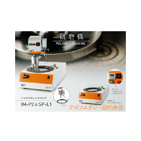
Presentation of Materials: Comprehensive Catalog of Grinding Machines for Integrated Production from Design to Assembly / IMT Corporation
IMT Corporation is a precision grinding equipment manufacturer headquartered in Wakayama. We previously had sales offices in Tokyo, Osaka, and Nagoya, but we have now decided to finally expand into Kyushu. Our company has been providing production equipment for the semiconductor and liquid crystal panel industries, as well as equipment for preparing materials for microscopic observation, for many years. Through our "domestic sample grinding machines" and "consumables for microscope sample preparation and grinding materials," we will consult on our customers' quality assurance operations. 【Features】 - Consistent support: A comprehensive production system from design to assembly in-house - Speedy response: Detailed and prompt service *For more details, please download the materials or contact us directly.

This is a new silicon wafer edge polishing device developed with the concept of space-saving and high throughput.
- Wafer processing/polishing equipment

Perfect for creating high-precision samples! We are currently giving away a technical book that reveals the best polishing conditions, leading to process reduction and improved accuracy!!


- Wafer processing/polishing equipment

Meticulous work unique to Japanese manufacturers! Detailed follow-up visits by sales representatives even after installation.

- Wafer processing/polishing equipment
![[Column] Episode 1 Part 1 - Everyth...](https://image.mono.ipros.com/public/product/image/754/2000844313/IPROS87243123240253513930.jpeg?w=280&h=280)
I'm graduating from hand polishing!
- Wafer processing/polishing equipment
![[Column] Episode 1 Part 2 - Everyth...](https://image.mono.ipros.com/public/product/image/2e2/2000844332/IPROS13307731317786019679.jpeg?w=280&h=280)
I'm graduating from hand polishing!
- Wafer processing/polishing equipment
![[Column] Episode 2 Part 1 - Solve t...](https://image.mono.ipros.com/public/product/image/a5e/2000894172/IPROS07313810911026506019.jpeg?w=280&h=280)
~Me, Polishing, and IMT~
- Wafer processing/polishing equipment
![[Column] Episode 2 Part 2 - Solve t...](https://image.mono.ipros.com/public/product/image/43c/2000894173/IPROS92238813014816664627.jpeg?w=280&h=280)
~Me, Kenma, and IMT~
- Wafer processing/polishing equipment

Realization of low Ra using high-quality grinding tape.
- Wafer processing/polishing equipment

[Made in Japan] Precision Grinding Tape Used
- Wafer processing/polishing equipment

Ideal for high-precision sample preparation! We also propose optimal polishing conditions! Reliable domestic machines with comprehensive after-sales support!


- Wafer processing/polishing equipment
![[Introduction] Sample Lab Center](https://image.mono.ipros.com/public/product/image/3bb/2000721861/IPROS98872278153279056483.png?w=280&h=280)
We will make proposals centered around polishing machines, polishing devices, and sample polishing machines, utilizing the know-how of all precision polishing technologies.


- Wafer processing/polishing equipment

Production of holders that meet your requests! We can create holders that respond to customer needs based on in-house design, and we are also capable of producing special shapes such as porous types a...


- Wafer processing/polishing equipment

Contributing to the simplification of inspection tasks with air-free semi-automatic polishing.


- Wafer processing/polishing equipment
![[Column] Episode 3 Part 1 - Manual ...](https://image.mono.ipros.com/public/product/image/51a/2000939251/IPROS69540763987577600618.jpeg?w=280&h=280)
~Me, Kenma, and IMT~
- Wafer processing/polishing equipment
![[Column] Episode 3 Part 2 - Manual ...](https://image.mono.ipros.com/public/product/image/159/2000939252/IPROS28817244719473077497.jpeg?w=280&h=280)
~Me, Kenma, and IMT~
- Wafer processing/polishing equipment
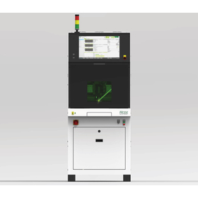

An innovative technology that heats the bond, making it easier to wedge bond copper wire.
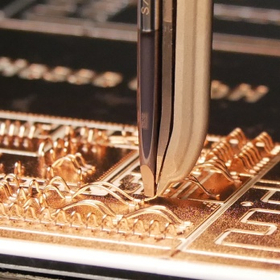
- Bonding Equipment

A controllable current transducer and frequency that continuously monitors wire deformation.
- Bonding Equipment

Expansion of productivity! The large work area allows for batch processing of multiple devices.
- Bonding Equipment

Dual-head wedge bonder for high-speed, high-precision, and high-productivity lead frames.
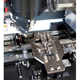
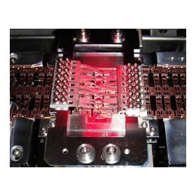
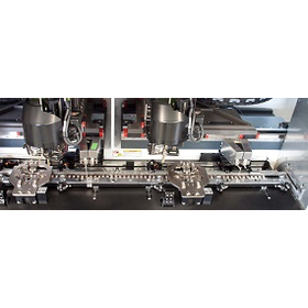
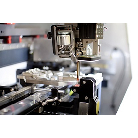
- Bonding Equipment
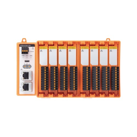

Modular remote I/O coupler unit that can efficiently configure the number of I/O points supported by EtherNet/IP.
- Other semiconductor manufacturing equipment
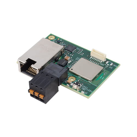
Modular remote I/O coupler unit that can efficiently configure the number of I/O points supported by EtherNet/IP.
- Other semiconductor manufacturing equipment


Measures against foreign matter contamination on the manufacturing line! It reliably removes foreign substances from the surface of the base material!
- label
- Coater
- Bag making machine/slitter


High-precision measurement of dew point, temperature and humidity, wind speed, and oxygen. Numerous compact models that are easy to integrate into devices! Ensures long-term stability for semiconducto...
- Sensors
- Sensors
- Other semiconductor manufacturing equipment
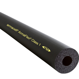

The embedded vapor barrier reduces the risk of corrosion under insulation (CUI).
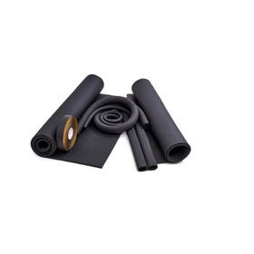
- Piping Materials
- Semiconductor inspection/test equipment
- Other semiconductor manufacturing equipment
![[Semiconductor/Wafer Inspection] AI...](https://image.mono.ipros.com/public/product/image/2009087/IPROS10607066819809733241.jpg?w=280&h=280)

For manufacturing sites troubled by excessive detection. This inspection device accurately determines fine defects in wafers through AI analysis and full-color image inspection, achieving improved yie...
- Semiconductor inspection/test equipment
- Wafer
- Circuit Board Inspection Equipment


This is a lineup of devices incorporating Rise One's precision transfer technology.
- Other semiconductor manufacturing equipment