
List of Semiconductor Manufacturing Equipment products
- classification:Semiconductor Manufacturing Equipment
946~990 item / All 5153 items


Reduce the workload from handling heavy objects! Here are five case studies that solved customer challenges! We are also accepting free consultations and tests tailored to your work!

- Other conveying machines


Strong cold wind from room temperature to -13°C! Depending on the usage environment, you can choose between the combo type or the separate type!
- Cooling system

April 10, 2024 (Wednesday) to April 12, 2024 (Friday) Notice of Participation in Nagoya Manufacturing World 2024
Sanwa Shiki Ventilator Co., Ltd. will be exhibiting at the 2024 Monozukuri World (Nagoya) held at Port Messe Nagoya. We will also be showcasing our large cooling fans and cool/warm ambient products. Date: April 10, 2024 - April 12, 2024 Opening: 10:00 AM Location: Nagoya Port Messe (Exhibition Hall 1) *Our booth: 19-1 We would be grateful if you could visit us if you have the time.


Simultaneous processing of stainless materials such as SUS316 using CNC lathes and machining centers. Manufacturing high-precision ring parts for semiconductor production.
- Other semiconductor manufacturing equipment
- Processing Contract


Flagship model: A handler that thoroughly pursues excellent stability and significant reductions in working time.
- Semiconductor inspection/test equipment
- Circuit Board Inspection Equipment
- Testing Equipment and Devices


Meeting the high cleanliness standards required in the semiconductor and medical device fields. We carry out everything from precision cleaning to packaging and assembly in a consistent clean environm...
- CVD Equipment
- Sputtering Equipment
- Resist Device

Pre-treatment for metal structure inspection will be carried out due to surface corrosion caused by chemicals.
- Other services
- Processing Contract
- Etching Equipment
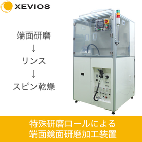

Polishing equipment (Edge Polish) that performs mirror polishing, rough polishing, and cleaning using filtered water and pure water as the medium without slurry.
- Other semiconductor manufacturing equipment


Flexibility, compact design, and low investment costs! An ideal choice for small-scale production.
- Sputtering Equipment
- Etching Equipment
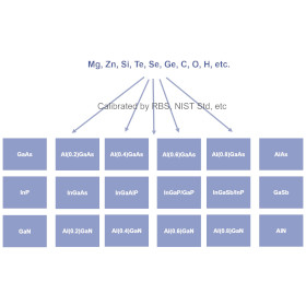

Correction of sensitivity coefficients and sputtering rates across all depths in response to changes in the sample matrix, enabling high-precision depth profile analysis.
- Contract Analysis
- Secondary ion mass spectrometer
- Ion implantation equipment
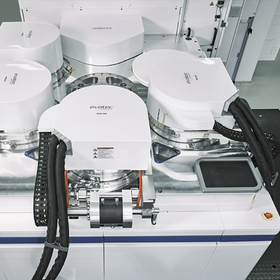
Extremely low Rc system design in the industry and the highest level of inter-wafer reproducibility!
- Sputtering Equipment
- Etching Equipment
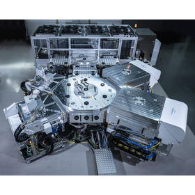
Higher productivity for PLP! More process possibilities. Optimized for advanced packaging.
- Sputtering Equipment
- Etching Equipment
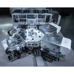
Evatec officially enters the next-generation packaging market in Japan with CLUSTERLINE 600 - Expanding business development towards the era of Panel-Level Packaging for AI and HPC.
Evatec AG (headquartered in Switzerland) is intensifying the deployment of its large panel-compatible coating platform "CLUSTERLINE 600" in the Japanese market and will fully enter the rapidly growing next-generation packaging market for AI (artificial intelligence) and high-performance computing (HPC). In the global semiconductor ecosystem, the transition to new manufacturing architectures such as large interposers, ultra-high-density RDL (Redistribution Layer), glass core substrates, and panel-level packaging is accelerating. In particular, with the increasing size of AI packages, the shift from traditional 300mm wafer-based manufacturing to 600mm class panel processes is gaining attention as a next-generation manufacturing technology. Evatec positions this change as one of the most important growth opportunities in the semiconductor industry over the next decade. By making the CLUSTERLINE 600 its core product, the company aims to expand its advanced packaging business in the Japanese market and support customers' technology development and mass production in areas such as panel-level packaging, advanced IC substrates, and glass core substrates.
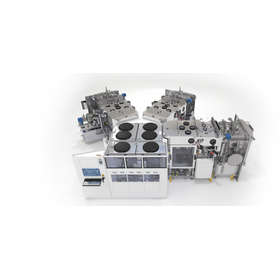
Introducing the BAK deposition platform that allows for various chamber sizes and process automation options.
- Evaporation Equipment


A unique LED UV curing solution with numerous patents obtained! Applying UV resin curing in electronics, industry, medical, and optics!
- Other semiconductor manufacturing equipment
- LED Module
- Ultraviolet irradiation equipment
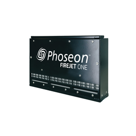
Expanding UV LED products to strengthen response to the growing and diversifying needs for ultraviolet curing.
Excelsius Noble Light Japan Co., Ltd. (Headquarters: Bunkyo-ku, Tokyo, President: Masahiko Suzuki, hereinafter referred to as "the Company") will expand its product portfolio of UV LEDs, one of the light sources for UV curing, and strengthen the provision of UV curing process solutions in new growth areas. In January 2024, the Company was absorbed by Excelsius Technologies, headquartered in the United States (hereinafter referred to as "Excelsius"), and is now handling UV LED products previously managed by its predecessor, Heraeus Noblelight Japan Co., Ltd., and Foseon Technology Japan Co., Ltd., as well as Excelsius. These products encompass a wide range of UV LED light sources for line and area irradiation as well as spot irradiation, regardless of cooling methods. As market demands become increasingly diverse, the Company has established a system that enables more detailed proposals to a broad range of industries through this product expansion.


Achieving thin film coating in micrometer units with a coater head (slot coat) application device.
- Coater

Used for temporary fixing and bonding with hot melt adhesive!
- Molding Equipment


We provide high-quality circuit processing and wiring processing services using FIB. We achieve a high processing yield!
- Semiconductor inspection/test equipment
- Semiconductors and ICs
- Microcomputer

Supply disruptions from semiconductor manufacturers, the electrification of the automotive industry, and the spread of 5G communication. Are you keeping up with the urgent need for alternative product evaluations, authenticity assessments, and failure analysis?
The spread of 5G communication, the electrification of the automotive industry, the intensification of US-China trade friction represented by certain semiconductor manufacturers leading to supply stoppages, and the rapid increase in digital products due to the impact of the COVID-19 pandemic are various social phenomena that are increasing the demand for semiconductors. Along with these developments, the acceleration of semiconductor supply risks is progressing. In addition to the adoption of new products, evaluation of existing and distributed products is also necessary... However, the personnel involved in new adoption and product evaluation are limited. Do you have any of these concerns? - Lack of know-how to evaluate semiconductor components - Want to evaluate alternative products but lack personnel and equipment - Want to use stock items and market products but have concerns about reliability - Unable to determine whether the delivered semiconductor products are counterfeit or genuine At Eurofins FQL, we leverage our years of experience in component evaluation and failure analysis to provide not only semiconductor evaluations but also failure analysis services. Additionally, we offer evaluations of distributed products to assist in determining the authenticity of counterfeit, imitation, or long-term stored items. Please feel free to contact us.

Processing S45C quenched and tempered steel using high-precision CNC machining technology. Manufacturing ring components for semiconductor manufacturing equipment.
- Other semiconductor manufacturing equipment
- Processing Contract

Using SUS304 stainless steel and utilizing NC lathes, machining centers, and cylindrical grinding, we manufacture high-precision ring components for semiconductor manufacturing equipment.
- Other semiconductor manufacturing equipment
- Processing Contract


Handling electronic assembly products such as solder balances and stirrers, as well as soldering equipment and semiconductor devices!
- Soldering Equipment
- Other semiconductor manufacturing equipment


Inspection is possible only on the surface of the double-sided implementation substrate! Also compatible with 3D tomography inspection. *Detailed explanatory materials will be provided.
- Semiconductor inspection/test equipment
- X-ray inspection equipment

Automatically inspect crystal defect voids inside silicon wafers!
- Semiconductor inspection/test equipment
- X-ray inspection equipment

X-ray observation device for analysis with a high resolution of 0.25 μm focal spot size.
- Semiconductor inspection/test equipment
- X-ray inspection equipment

Automated X-ray inspection device for inspecting solder bumps on wafers.
- Semiconductor inspection/test equipment
- X-ray inspection equipment
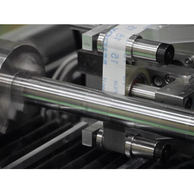

Automation of super finishing processes and uniformity of roughness. We propose polishing equipment for outer diameter, inner diameter, end face, etc., tailored to your applications and shapes.
- Wafer processing/polishing equipment


Highly versatile! Guarantees a shining edge, perfect finish, and short processing time.
- Wafer processing/polishing equipment

A highly versatile fully electric solution for flat and shaped edges!
- Wafer processing/polishing equipment

Guaranteed high-quality finish and consistent performance! Stone grinding machine with excellent output.
- Wafer processing/polishing equipment
- Stone Processing Machinery

Vivid in the vertical direction! Precisely vertically polished straight edges of marble and granite.
- Wafer processing/polishing equipment

Unique solutions for precision, efficiency, and reliability in stone polishing.
- Wafer processing/polishing equipment
- Stone Processing Machinery


High-precision inspection equipment compatible with transparent materials.
- Semiconductor inspection/test equipment

[Exhibition Information] We will be exhibiting at 'SEMICON JAPAN 2025'.
We will be exhibiting Kubota's semiconductor inspection equipment at SEMICON JAPAN, an international exhibition of manufacturing technologies, equipment, and materials in the semiconductor industry. All of our staff sincerely look forward to your visit. 【Exhibition Information】 Date: December 17 (Wed) - 19 (Fri), 2025, 10:00 - 17:00 Venue: Tokyo Big Sight Booth Location: W1963 *Advance registration is required for attendance. Please check the SEMICON JAPAN website for registration details.

Automating visual inspection of wafer defects.
- Semiconductor inspection/test equipment
[Exhibition Information] We will be exhibiting at 'SEMICON JAPAN 2025'.
We will be exhibiting Kubota's semiconductor inspection equipment at SEMICON JAPAN, an international exhibition of manufacturing technologies, equipment, and materials in the semiconductor industry. All of our staff sincerely look forward to your visit. 【Exhibition Information】 Date: December 17 (Wed) - 19 (Fri), 2025, 10:00 - 17:00 Venue: Tokyo Big Sight Booth Location: W1963 *Advance registration is required for attendance. Please check the SEMICON JAPAN website for registration details.

Equipped with a review microscope! Defects detected can be observed in real-time with the microscope.
- Semiconductor inspection/test equipment
[Exhibition Information] We will be exhibiting at 'SEMICON JAPAN 2025'.
We will be exhibiting Kubota's semiconductor inspection equipment at SEMICON JAPAN, an international exhibition of manufacturing technologies, equipment, and materials in the semiconductor industry. All of our staff sincerely look forward to your visit. 【Exhibition Information】 Date: December 17 (Wed) - 19 (Fri), 2025, 10:00 - 17:00 Venue: Tokyo Big Sight Booth Location: W1963 *Advance registration is required for attendance. Please check the SEMICON JAPAN website for registration details.


Tabletop conveyor. How about for simple verification of fine parts?
- Image Processing Equipment
- Other semiconductor manufacturing equipment

3D Inspection Device HISR - Assisting with precise inspection and verification.


- Color camera
- Other semiconductor manufacturing equipment


We have achievements such as 'sputtering equipment with GB for organic EL' and 'IBS equipment for research and development'!


- Sputtering Equipment

We have a track record of equipment such as 'plasma CVD systems for metal containers' and 'ICP-type MOCVD systems'!


- CVD Equipment

Supports tray transport! Achieves excellent substrate temperature distribution and gas flow method.

- Annealing furnace
- Heating device

Switching between RIE mode and DP mode is possible! Reduction of metal contamination through special surface treatment.
- Etching Equipment

Reduction of particles through suitable surface treatment! Compatible with high vacuum processes using a load-lock system.
- Evaporation Equipment

We have a track record of devices such as the "two-stage composite Pt deposition system"! Please contact us when you need assistance.


- Evaporation Equipment

You can freely choose from the plasma cleaning chamber, organic deposition chamber, electrode deposition chamber, sealing chamber, and more!


- Evaporation Equipment

Maximum substrate heating temperature of 1000℃! Reduces element loss specific to the substrate surface heating process!

- Heating device
- Annealing furnace

It is a versatile and compact device that enables etching, ashing, and ion cleaning!
- Etching Equipment
- Ashing device

Demo units available for loan! Ideal for spin drying silicon wafers, masks, and film substrates!
- Other clean room equipment and facilities
- Other semiconductor manufacturing equipment

Demo units available for loan! This is a cassette-type batch cleaning device that can accommodate up to Φ300.
- Other semiconductor manufacturing equipment