
List of Semiconductor inspection/test equipment products
- classification:Semiconductor inspection/test equipment
136~180 item / All 749 items


We provide comprehensive support from design to manufacturing and maintenance!


- Contract manufacturing


It won't break even after 1 million repetitions! A mat switch with reliable operation, high durability, and low price. Suitable for options in machine tools as well. Please consult us about delivery t...
- Sensors


It is a device that removes impurities attached to high-purity gas cylinders used in semiconductor manufacturing processes.
- Semiconductor inspection/test equipment


266nm CW (continuous wave) laser 10mW - 550mW @ 266nm Compact head Air-cooled, low noise
- Semiconductor inspection/test equipment


Introducing a 21-megapixel CoaXPress-over-Fiber (CoF) camera that supports image transmission at up to 100 Gbps!
- Semiconductor inspection/test equipment


Customize the optical integrated circuit you want to measure! It can also be used for spectral analysis and functional testing.


- Semiconductor inspection/test equipment


We have various types available, including high-load types and those that can be fixed to walls.
- Workstation
- Semiconductor inspection/test equipment
- Desktop PC


We provide development and design technology for heating furnaces and heating systems with 30 years of experience in drawing furnaces and vitrification furnaces for optical fibers.
- Industrial Furnace
- Electric furnace
- Semiconductor inspection/test equipment


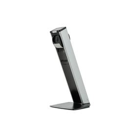
Significant cost reduction for AI appearance inspection systems!! A starter set that can be introduced more easily, more simply, and in a short period of time.


- Visual Inspection Equipment
- Semiconductor inspection/test equipment
- Inspection fixture
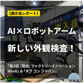
[Exhibition Report] New Appearance Inspection Showcased by AI x Robot Arm! "2nd [Kansai] Factory Innovation Week" & "Nepcon Japan"
This time, we will deliver a local report on the "2nd [Kansai] Factory Innovation Week," held from May 13 (Wednesday) to 15 (Friday), 2026, at Intex Osaka, along with the concurrently held "2nd [Kansai] Nepcon Japan"! As one of the largest manufacturing exhibitions in Kansai, the venue was filled with the enthusiasm of engineers and business leaders seeking the latest technologies. This time, we will particularly focus on the highlights of the exhibition, centering around the latest solutions utilizing "robot arms + cameras," which caught the eye at the venue!


Analyze industry and market trends in semiconductors, focusing on chiplet technology, advanced packaging technology, chiplet packaging technologies, materials, and equipment configuration!
- Other semiconductors
- Other semiconductor manufacturing equipment
- Semiconductor inspection/test equipment
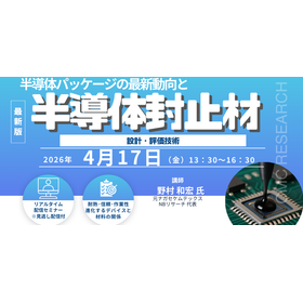
Web Seminar on "Latest Trends in Semiconductor Packaging and Semiconductor Encapsulation Materials" on April 17
■Title: "Latest Trends in Semiconductor Packaging and Design/Evaluation Techniques for Semiconductor Encapsulation Materials" ――As chipletization and 3D packaging advance in semiconductors, more sophisticated material design for encapsulants is required than ever before. This seminar will provide a detailed practical perspective on the latest trends in semiconductor packaging, covering raw material selection, design techniques, and reliability evaluation of encapsulants. ■Date and Time: April 17, 2026 (Friday) 13:30–16:30 ■Target Audience: Designers of semiconductor encapsulation materials, engineers using semiconductor encapsulation materials, designers of epoxy resins and hardeners for semiconductor encapsulation materials ■Knowledge Gained from the Seminar: - Trends in semiconductor packaging - Knowledge about raw materials for semiconductor encapsulation materials - Design techniques for semiconductor encapsulation materials and evaluation techniques for semiconductor encapsulation materials
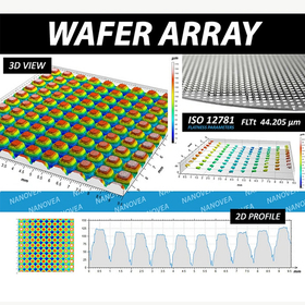

Introducing various application notes for semiconductor strength testing, surface inspection, environmental testing, and more.
- Wafer
- Semiconductor inspection/test equipment
- Other semiconductors

Introduction to Theoretical Analysis of Wire Probe Wear
- probe
- Tester
- Semiconductor inspection/test equipment


Techno Alpha is the Japanese distributor of K&S wire bonders, which boasts a top-class global share in wire bonding, as well as consumables for wire bonders.


- Bonding Equipment
- Other semiconductor manufacturing equipment
- Semiconductor inspection/test equipment

High-speed line inspection at SWIR 2K×1, 110kHz
- Monochrome camera
- Semiconductor inspection/test equipment
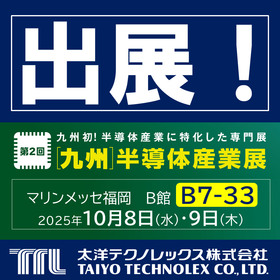

Full support from FPC design, prototyping, and mass production to board power-on testing, appearance inspection systems, and FA automation! TAIYO FPC SOLUTIONS!
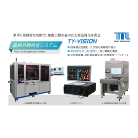

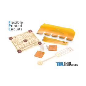
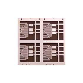
- Semiconductor inspection/test equipment
- Printed Circuit Board
- Circuit board design and manufacturing
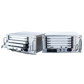

High Cost Performance Mixed Signal Tester
- Semiconductor inspection/test equipment


Leave silicon carbide and silicon nitride to JFC.
- Fine Ceramics
- Other machine elements
- Semiconductor inspection/test equipment

Exhibited at the 2017 High-Performance Ceramics Exhibition at Tokyo Big Sight from April 5 to 7.
Thank you to everyone who visited us. We will be exhibiting at the "High-Performance Ceramics Exhibition" held at Tokyo Big Sight in April. At our booth, we will showcase: - A new product that further enhances the fracture resistance of silicon nitride ceramics and improves thermal conductivity. - A new material that does not bend like iron, utilizing the lightweight properties of aluminum, known as "composite materials of metals and ceramics." - "Ceramic substrates" characterized by thin film and film formation technology. If you have any concerns regarding equipment design, component design, thermal design, or anything else, please feel free to stop by our booth for a consultation. We look forward to seeing you.

High-end model: A handler that thoroughly pursues excellent stability and significant reduction in working hours.
- Semiconductor inspection/test equipment
- Tester

Flagship model: A handler that thoroughly pursues excellent stability and significant reductions in working time.
- Semiconductor inspection/test equipment
- Circuit Board Inspection Equipment
- Testing Equipment and Devices


We provide high-quality circuit processing and wiring processing services using FIB. We achieve a high processing yield!
- Semiconductor inspection/test equipment
- Semiconductors and ICs
- Microcomputer
Supply disruptions from semiconductor manufacturers, the electrification of the automotive industry, and the spread of 5G communication. Are you keeping up with the urgent need for alternative product evaluations, authenticity assessments, and failure analysis?
The spread of 5G communication, the electrification of the automotive industry, the intensification of US-China trade friction represented by certain semiconductor manufacturers leading to supply stoppages, and the rapid increase in digital products due to the impact of the COVID-19 pandemic are various social phenomena that are increasing the demand for semiconductors. Along with these developments, the acceleration of semiconductor supply risks is progressing. In addition to the adoption of new products, evaluation of existing and distributed products is also necessary... However, the personnel involved in new adoption and product evaluation are limited. Do you have any of these concerns? - Lack of know-how to evaluate semiconductor components - Want to evaluate alternative products but lack personnel and equipment - Want to use stock items and market products but have concerns about reliability - Unable to determine whether the delivered semiconductor products are counterfeit or genuine At Eurofins FQL, we leverage our years of experience in component evaluation and failure analysis to provide not only semiconductor evaluations but also failure analysis services. Additionally, we offer evaluations of distributed products to assist in determining the authenticity of counterfeit, imitation, or long-term stored items. Please feel free to contact us.


Inspection is possible only on the surface of the double-sided implementation substrate! Also compatible with 3D tomography inspection. *Detailed explanatory materials will be provided.
- Semiconductor inspection/test equipment
- X-ray inspection equipment

Automatically inspect crystal defect voids inside silicon wafers!
- Semiconductor inspection/test equipment
- X-ray inspection equipment

X-ray observation device for analysis with a high resolution of 0.25 μm focal spot size.
- Semiconductor inspection/test equipment
- X-ray inspection equipment

Automated X-ray inspection device for inspecting solder bumps on wafers.
- Semiconductor inspection/test equipment
- X-ray inspection equipment


High-precision inspection equipment compatible with transparent materials.
- Semiconductor inspection/test equipment

[Exhibition Information] We will be exhibiting at 'SEMICON JAPAN 2025'.
We will be exhibiting Kubota's semiconductor inspection equipment at SEMICON JAPAN, an international exhibition of manufacturing technologies, equipment, and materials in the semiconductor industry. All of our staff sincerely look forward to your visit. 【Exhibition Information】 Date: December 17 (Wed) - 19 (Fri), 2025, 10:00 - 17:00 Venue: Tokyo Big Sight Booth Location: W1963 *Advance registration is required for attendance. Please check the SEMICON JAPAN website for registration details.

Automating visual inspection of wafer defects.
- Semiconductor inspection/test equipment
[Exhibition Information] We will be exhibiting at 'SEMICON JAPAN 2025'.
We will be exhibiting Kubota's semiconductor inspection equipment at SEMICON JAPAN, an international exhibition of manufacturing technologies, equipment, and materials in the semiconductor industry. All of our staff sincerely look forward to your visit. 【Exhibition Information】 Date: December 17 (Wed) - 19 (Fri), 2025, 10:00 - 17:00 Venue: Tokyo Big Sight Booth Location: W1963 *Advance registration is required for attendance. Please check the SEMICON JAPAN website for registration details.

Equipped with a review microscope! Defects detected can be observed in real-time with the microscope.
- Semiconductor inspection/test equipment
[Exhibition Information] We will be exhibiting at 'SEMICON JAPAN 2025'.
We will be exhibiting Kubota's semiconductor inspection equipment at SEMICON JAPAN, an international exhibition of manufacturing technologies, equipment, and materials in the semiconductor industry. All of our staff sincerely look forward to your visit. 【Exhibition Information】 Date: December 17 (Wed) - 19 (Fri), 2025, 10:00 - 17:00 Venue: Tokyo Big Sight Booth Location: W1963 *Advance registration is required for attendance. Please check the SEMICON JAPAN website for registration details.


~Easily choose specifications on the web~ Semi-order porous chuck
- Semiconductor inspection/test equipment

A new pixel-shifting SWIR camera capable of high-resolution (5M, 12M, 21M) imaging in the SWIR band and applicable for various inspection purposes has arrived!

- Semiconductor inspection/test equipment
- Monochrome camera
- Color camera

Introducing a 21-megapixel CoaXPress-over-Fiber (CoF) camera that supports image transmission at up to 425 fps!
- Semiconductor inspection/test equipment

Compact, lightweight, and low-cost! The CXP interface enables high frame rates and long-distance transmission.
- Semiconductor inspection/test equipment

【NEW!】CIS Product Comprehensive Catalog【March 2020】
A variety of cameras are packed with features such as compact size, high speed, high image quality, high resolution, the adoption of new interfaces, and the inclusion of a CIS original image processing engine! [Contents of this issue] ■ CoaXpress cameras ■ CameraLink cameras ■ Pixel-shift cameras ■ Board cameras (GigE/USB3.0) ■ Accessories ■ Semi-custom lenses ■ Cameras equipped with our proprietary technology "Clairvu" ■ Case studies on image processing system development In addition to the models that have been well-received so far, we are excited to introduce new products: "50M high-resolution CXP camera," "25M high-speed CXP camera," "RGB+Depth information acquisition capable USB3.0 I/F ToF camera development kit," "4K high-speed Clairvu-equipped camera," and "4K camera with 18x zoom lens and Clairvu." There is a wide range of cameras suitable for various industrial applications such as traffic monitoring, broadcasting, medical, heavy steel plants, logistics, robot vision, and various inspections. Please take a look at the enhanced lineup of CIS cameras! *For more detailed information or to request an English version of the catalog, please contact our sales department.

Ideal for FA applications such as substrate and appearance inspection. A camera series that is compact, high-resolution, low-cost, capable of high frame rates, long-distance transmission, and multi-ch...

- Semiconductor inspection/test equipment
【NEW!】CIS Product Comprehensive Catalog【March 2020】
A variety of cameras are packed with features such as compact size, high speed, high image quality, high resolution, the adoption of new interfaces, and the inclusion of a CIS original image processing engine! [Contents of this issue] ■ CoaXpress cameras ■ CameraLink cameras ■ Pixel-shift cameras ■ Board cameras (GigE/USB3.0) ■ Accessories ■ Semi-custom lenses ■ Cameras equipped with our proprietary technology "Clairvu" ■ Case studies on image processing system development In addition to the models that have been well-received so far, we are excited to introduce new products: "50M high-resolution CXP camera," "25M high-speed CXP camera," "RGB+Depth information acquisition capable USB3.0 I/F ToF camera development kit," "4K high-speed Clairvu-equipped camera," and "4K camera with 18x zoom lens and Clairvu." There is a wide range of cameras suitable for various industrial applications such as traffic monitoring, broadcasting, medical, heavy steel plants, logistics, robot vision, and various inspections. Please take a look at the enhanced lineup of CIS cameras! *For more detailed information or to request an English version of the catalog, please contact our sales department.


We will propose solutions in the semiconductor field, which we specialize in, tailored to our customers' needs!


- Other microscopes
- Resist Device
- Semiconductor inspection/test equipment


We will handle everything from the evaluation of the diffusion layer to physical analysis/chemical analysis regarding the malfunctioning part!


- Analysis Services
- Contract Analysis
- Semiconductor inspection/test equipment

Announcement of the introduction of Talos F200E
Our company will introduce the FEI "Talos F200E" transmission electron microscope system. Compared to conventional models, the resolution for TEM and STEM has improved, and performance has been significantly enhanced, allowing for EDS analysis with four detectors. Additionally, it is equipped with features such as drift-corrected frame integration (DCFI), which accumulates multiple frames while correcting for drift.

Back grinding is possible with various types of semiconductors! You can observe the elements and the condition of defects.


- Analysis Services
- Semiconductor inspection/test equipment


We leverage our expertise in hydraulic, pneumatic, and electrical technologies to propose and provide solutions that align with our customers' needs.
- Assembly Machine
- Semiconductor inspection/test equipment
- Transport and handling robots

We leverage our expertise in hydraulics, pneumatics, and electrical technology to propose and provide solutions that align with our customers' needs.
- Assembly Machine
- Semiconductor inspection/test equipment
- Transport and handling robots