We have compiled a list of manufacturers, distributors, product information, reference prices, and rankings for microscope.
ipros is IPROS GMS IPROS One of the largest technical database sites in Japan that collects information on.

microscope(afm) - List of Manufacturers, Suppliers, Companies and Products | IPROS GMS

Last Updated: Aggregation Period:Mar 11, 2026~Apr 07, 2026
This ranking is based on the number of page views on our site.

microscope Product List

1~30 item / All 59 items

Displayed results

AFM platform with optical microscope

Achieves high-speed scanning and high resolution imaging using atomic force microscopy. Compatible with measurements in air and liquid.

This is an AFM platform equipped with an optical microscope. It allows imaging with an atomic force microscope targeting areas observed with the optical microscope. It adopts a vertical optical path design, and the gas-liquid dual-use probe holder can be used simultaneously in both air and liquid. (Liquid measurement option required) *For more details, please contact us.*

  • probe
  • microscope

Added to bookmarks

Bookmarks list

Bookmark has been removed

Bookmarks list

You can't add any more bookmarks

By registering as a member, you can increase the number of bookmarks you can save and organize them with labels.

Free membership registration

AFM Data Collection

AFM: Atomic Force Microscopy Method

AFM is a method that scans the surface of a sample with a fine probe and measures nano-scale surface topography in three dimensions. It can measure a wide range of materials, not only for the evaluation of metals, semiconductors, and oxides, but also for soft materials such as hair and contact lenses. This document presents various AFM images of different materials.

Added to bookmarks

Bookmarks list

Bookmark has been removed

Bookmarks list

You can't add any more bookmarks

By registering as a member, you can increase the number of bookmarks you can save and organize them with labels.

Free membership registration

Data DL available: AFM Case Studies in Scanning Probe Microscopy

We will introduce numerous analysis cases using AFM scanning probe microscopy, such as structural analysis, elastic modulus measurement, and conductivity measurement.

In this case study collection, we will introduce analysis examples using "AFM: Scanning Probe Microscopy." [Contents] ● Method and results of "Structural analysis and elastic modulus measurement of food (somen)" ● Features and analysis examples of "Conductive measurements of AFM in a vacuum" ● Features and analysis examples of "Conductivity evaluation of material surfaces using AFM" ● "AFM observation of polymer materials (smoothing by microtome)" We conduct various analyses using AFM, which is one of our strengths. We hope you will take a look. There are many other examples not included here. *For more details, please refer to our other PDF materials or feel free to contact us.

  • Other microscopes
  • Contract Analysis
  • Surface treatment contract service
  • microscope

Added to bookmarks

Bookmarks list

Bookmark has been removed

Bookmarks list

You can't add any more bookmarks

By registering as a member, you can increase the number of bookmarks you can save and organize them with labels.

Free membership registration

AFM Atomic Force Microscope Nano Observer 2

Achieving measurement quality comparable to high-end products from established AFM manufacturers.

Combining flexibility, outstanding performance, and user-friendly operability, it achieves measurement quality comparable to high-end products from established AFM manufacturers. It is equipped with a wide range of functions for nanoscale imaging and characterization. It also enables electrical property measurements (KFM, C-AFM) and features a soft IC mode that can measure fragile samples.

  • Other microscopes
  • microscope

Added to bookmarks

Bookmarks list

Bookmark has been removed

Bookmarks list

You can't add any more bookmarks

By registering as a member, you can increase the number of bookmarks you can save and organize them with labels.

Free membership registration

AFM-IR device with sub-5 nm IR spatial resolution

AFM-IR device Spectroscopic Nanoscopy PiFM・PiF-IR

This is an AFM-IR device that achieves sub-5 nm IR spatial resolution. It is a compact and self-contained system. The optical system allows for easy quick change and switching, and access to the sample is straightforward.

  • Other microscopes
  • microscope

Added to bookmarks

Bookmarks list

Bookmark has been removed

Bookmarks list

You can't add any more bookmarks

By registering as a member, you can increase the number of bookmarks you can save and organize them with labels.

Free membership registration

[Application Example] Atomic Force Microscopy (AFM) Experiment

The 8-channel Spectrum DigitizerNETBOX provides the high precision necessary to drive the evolution of AFM. Comes with a comprehensive catalog.

I would like to introduce an application example of Atomic Force Microscopy (AFM) experiments at the Precision Mechatronics Laboratory of Newcastle University, UK. Atomic Force Microscopy is an important tool in materials science and is used for mechanical scanning of surfaces. The forces acting between the surface atoms and the tip of the nanoscale probe are measured and calculated, achieving a resolution on the order of a fraction of a nanometer. [Overview] ■ AFM Technology ■ High-precision Multi-channel Digitizer *For more details, please feel free to contact us.

  • Other electronic parts
  • microscope

Added to bookmarks

Bookmarks list

Bookmark has been removed

Bookmarks list

You can't add any more bookmarks

By registering as a member, you can increase the number of bookmarks you can save and organize them with labels.

Free membership registration

[Analysis Case] Dynamic Viscoelastic Evaluation of PDMS using AFM

Introduction to the evaluation of in-plane distribution of viscoelasticity and frequency dependence!

Our organization offers dynamic viscoelastic evaluation of PDMS using AFM. Dynamic Mechanical Analysis (DMA) is an effective method for investigating viscoelastic behavior, which is an important factor in the research and development of polymer materials. Additionally, by combining it with the AFM mechanism, it becomes possible to measure in-plane distribution and evaluate localized areas. This document presents a case study using AFM-DMA to map the viscoelastic modulus of PDMS (polydimethylsiloxane) and conduct frequency-dependent spectroscopy evaluation. [Measurement Method / Processing Method] ■ [AFM] Atomic Force Microscopy *For more details, please download the PDF or feel free to contact us.

Added to bookmarks

Bookmarks list

Bookmark has been removed

Bookmarks list

You can't add any more bookmarks

By registering as a member, you can increase the number of bookmarks you can save and organize them with labels.

Free membership registration

Custom Atomic Force Microscope (AFM) System

We will design and build a customized AFM system tailored to your needs!

It is necessary to conduct AFM measurements, but does the sample require special handling due to its size, or does it require experiments that differ from conventional techniques and methods? We sincerely take your needs into consideration and will work together with you to find solutions. At Japan Quantum Design, we design and build systems tailored to your requirements through close collaboration with the device development team at Nanosurf, the manufacturer based in Switzerland. If you have any concerns or requests regarding surface measurements, please feel free to contact us!

  • Other measurement, recording and measuring instruments
  • microscope

Added to bookmarks

Bookmarks list

Bookmark has been removed

Bookmarks list

You can't add any more bookmarks

By registering as a member, you can increase the number of bookmarks you can save and organize them with labels.

Free membership registration

AFM/SPM for Polymers Cypher ES Polymer Edition

Standard-equipped with optimal measurement modes and options for polymer material research! Atomic force microscope for polymers based on ultra-high-performance environment-controlled AFM/SPM.

The Cypher ES Polymer Edition is based on the Cypher ES, which adds sophisticated environmental control to Asylum Research's ultra-high-performance AFM, and comes standard with measurement modes and options that are optimal for polymer materials research and polymer characterization (see "Basic Information" below). ● For other features and details, please refer to the catalog or contact us.

  • Other measurement, recording and measuring instruments
  • Microscope
  • microscope

Added to bookmarks

Bookmarks list

Bookmark has been removed

Bookmarks list

You can't add any more bookmarks

By registering as a member, you can increase the number of bookmarks you can save and organize them with labels.

Free membership registration

[Analysis Case] Evaluation of Mechanical Properties of Hair Cross-Sections Prepared by Microtome Method

It is possible to evaluate the elastic modulus of the internal structure of soft materials.

When evaluating the internal structure of materials, it is necessary to expose the internal structure while maintaining it through cross-sectional processing techniques such as cutting and polishing. This document introduces a case where the microtome method, which has a relatively small impact from processing damage, was used to create cross-sections of hair, followed by AFM observation of the internal structure and evaluation of elastic modulus. The microtome method is a cutting processing technique widely used in the field of soft materials, such as rubber materials and biological samples, and this approach has made it possible to evaluate the mechanical properties of the internal structure of these materials. [Measurement and Processing Methods] [AFM] Atomic Force Microscopy [AFM-MA・AFM-DMA] Mechanical Property Evaluation (Elastic Modulus Measurement, Dynamic Viscoelasticity Measurement) Ultra Microtome Processing *For more details, please download the PDF or feel free to contact us.

  • img_c0670_3_Microtome_Modulus_DMT_JKR_Hair_diagram.jpg
  • Contract measurement
  • Contract Analysis
  • microscope

Added to bookmarks

Bookmarks list

Bookmark has been removed

Bookmarks list

You can't add any more bookmarks

By registering as a member, you can increase the number of bookmarks you can save and organize them with labels.

Free membership registration

Conductivity evaluation of plated contact component surfaces 【DL available/AFM】

AFM can capture and measure extremely small surface topographies (roughness).

The AFM scanning probe microscope is a device that "detects various physical interactions between the probe and the sample surface, allowing for the observation of surface shapes in minute areas and the measurement of electrical and mechanical properties." These physical interactions include atomic forces, frictional forces, and electrostatic forces. Additionally, measurements can be taken in various environments, including atmospheric and vacuum conditions, enabling the observation of sample surfaces regardless of conductivity or insulation. Using this analytical device, we conducted an investigation into the "surface treatment of plated connector contact parts." Please take a moment to read the PDF materials. Furthermore, in addition to this analytical device, our company also conducts various surface analyses such as XPS, AES, and GD-OES. We would be happy to assist you, so please feel free to reach out. Seiko Future Creation Official Website https://www.seiko-sfc.co.jp/ *We have many other achievements as well. If you request through the inquiry button, we will send them to you.

  • Plating Equipment
  • Contract Analysis
  • Electrical Instruments/Electrometers
  • microscope

Added to bookmarks

Bookmarks list

Bookmark has been removed

Bookmarks list

You can't add any more bookmarks

By registering as a member, you can increase the number of bookmarks you can save and organize them with labels.

Free membership registration

High-speed atomic force microscope (high-speed AFM) 'MS-NEX'

Even those who are handling AFM for the first time can easily observe videos at the nanoscale!

The "MS-NEX" is a high-speed atomic force microscope (high-speed AFM) module system that allows for video observation of samples at the nanoscale and in real-time within a solution. It flexibly responds to requests such as "I need this function now" or "I won't use this function now." Depending on your research theme, progress, and budget, you can use a high-speed AFM that matches your current needs by combining various modules. 【Features】 ■ Capable of video observation at the nanoscale and in real-time ■ Various functions can be freely combined as needed ■ Modules can be added later ■ Equipped with various support functions ■ Easy to use even for those handling AFM for the first time *For more details, please refer to the PDF document or feel free to contact us.

  • Microscope
  • others
  • microscope

Added to bookmarks

Bookmarks list

Bookmark has been removed

Bookmarks list

You can't add any more bookmarks

By registering as a member, you can increase the number of bookmarks you can save and organize them with labels.

Free membership registration

Atomic Force Microscope (AFM) "Park NX-3DM"

Fully automated industrial AFM with NX technology implemented.

The "Park NX-3DM" is a fully automated AFM (Atomic Force Microscope) system designed for overhang profiling, high-resolution sidewall imaging, and critical angle measurement. With its patented separated XY and Z scanning system equipped with an inclined Z scanner, it overcomes the challenges of conventional and flare chip methods in accurate sidewall analysis. 【Essential Tool for Wafer Fabrication】 ■ Fully automated industrial AFM using advanced and precise Park NX technology ■ Tilt head design for undercut and overhang structures ■ Accurate sidewall roughness measurement without the need for sample pretreatment ■ High-quality images can be obtained without damaging the device or sample due to the fully non-contact mode (TM) *For more details, please download the PDF or feel free to contact us.

Added to bookmarks

Bookmarks list

Bookmark has been removed

Bookmarks list

You can't add any more bookmarks

By registering as a member, you can increase the number of bookmarks you can save and organize them with labels.

Free membership registration

Atomic Force Microscope (AFM) "Park NX10"

Atomic force microscope providing reliable data with the highest level of nanoscale resolution.

The "Park NX10" is an atomic force microscope (AFM) that can be easily operated at all stages, from sample setup to imaging, measurement, and analysis. With this product, users can focus more on innovative research based on better data and more time. 【Features】 ■ Accurate XY scanning without bowing due to crosstalk removal ■ Accurate AFM topography using a low-noise Z detector ■ Top-class chip lifespan, resolution, and sample protection with true non-contact (TM) mode ■ Nano-order surface analysis of various materials such as semiconductors, polymers, battery materials, and carbon-based materials (see image gallery) *For more details, please refer to the PDF document or feel free to contact us.

Added to bookmarks

Bookmarks list

Bookmark has been removed

Bookmarks list

You can't add any more bookmarks

By registering as a member, you can increase the number of bookmarks you can save and organize them with labels.

Free membership registration

Atomic Force Microscope (AFM) "Park NX12-Bio"

Powerful scanning probe microscope for life sciences

The "Park NX12-Bio" is an atomic force microscope (AFM) equipped with three types of high-performance nanoscale microscopes on a single innovative platform. It enables both innovative liquid imaging with scanning ion conductance microscopy (SICM) and the highly regarded atomic force microscopy (AFM) technology. 【Comprehensive Solution for Nanoscale Biological Research】 ■ Equipped with a fracture-type fully independent Z-axis scanner/XY scanner, featuring high-precision Park NX AFM with complete non-contact technology (TM) ■ Ultra-high-resolution optical imaging using inverted optical microscopy technology ■ Enhanced biological cell imaging through the integration of scanning ion conductance microscopy *For more details, please download the PDF or feel free to contact us.

Added to bookmarks

Bookmarks list

Bookmark has been removed

Bookmarks list

You can't add any more bookmarks

By registering as a member, you can increase the number of bookmarks you can save and organize them with labels.

Free membership registration

[Analysis Case] Observation of Hair Surface Microstructure by AFM

Quantitative evaluation with reduced alteration is possible through analysis in the atmosphere.

This case study introduces an analysis of the condition of the cuticle on the hair surface using AFM. AFM is a method for three-dimensional measurement of nanoscale surface roughness. Since the analysis is conducted in the atmosphere, it does not cause degradation or gas release of organic materials, allowing for an evaluation of the sample's original shape. In this case study, we assessed the degree of cuticle opening, the distribution of adhered substances, and the roughness evaluation of different areas through images, as well as quantitatively evaluated the surface roughness through numerical processing. This method is effective for evaluating the condition of hair after shampooing and the application state after applying styling products.

Added to bookmarks

Bookmarks list

Bookmark has been removed

Bookmarks list

You can't add any more bookmarks

By registering as a member, you can increase the number of bookmarks you can save and organize them with labels.

Free membership registration

[Data Download Available] Smoothing of Polymer Materials by Microtome and AFM Observation

High-resolution observation of soft polymer materials is possible with a cryo-microtome and AFM.

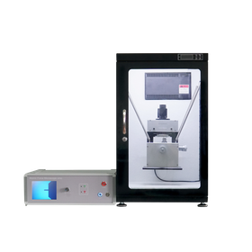
AFM scanning probe microscopy is a device that detects various physical interactions occurring between a probe and the sample surface, allowing for the observation of surface morphology in small areas and the measurement of electrical and mechanical properties. These physical interactions include atomic force, frictional force, and electrostatic force. It can perform measurements in various environments, including atmospheric and vacuum conditions, and is capable of observing sample surfaces regardless of whether they are conductive or insulating. Additionally, by using a cryo-microtome, it is possible to produce ultra-thin sections of soft polymer materials such as resins under frozen conditions. We are observing polyisoprene rubber from various angles using this AFM and cryo-microtome. Please take a moment to read the PDF materials. This technology can be applied not only to rubber but also to resins, plastics, and various polymer materials. Furthermore, our company conducts various surface analyses, including XPS, AES, and GD-OES, in addition to this analytical device. We would be happy to assist you, so please feel free to reach out. Seiko Future Creation Official Website https://www.seiko-sfc.co.jp/ *Other materials are also available. If you request through the inquiry button, we will send them to you.

  • Other polymer materials
  • Contract Analysis
  • Rubber
  • microscope

Added to bookmarks

Bookmarks list

Bookmark has been removed

Bookmarks list

You can't add any more bookmarks

By registering as a member, you can increase the number of bookmarks you can save and organize them with labels.

Free membership registration

[Analysis Case] AFM Analysis of Smartphone Protective Films

Quantitative evaluation of the quality of sensory products is possible.

The penetration rate of smartphones is increasing year by year, and along with that, the protective films applied to their surfaces are diversifying in functionality. In this instance, we will introduce a case where two types of films (A and B) with fingerprint prevention and anti-reflection features were quantitatively evaluated in terms of roughness, simulating the sensation of touch through AFM analysis.

  • サムネ.png
  • Contract Analysis
  • LCD display
  • microscope

Added to bookmarks

Bookmarks list

Bookmark has been removed

Bookmarks list

You can't add any more bookmarks

By registering as a member, you can increase the number of bookmarks you can save and organize them with labels.

Free membership registration

Environmentally controlled, ultra-high performance AFM/SPM Cypher ES

A model of the Cypher S, which boasts exceptional performance, with fully equipped enhanced environmental control features. It easily achieves temperature control, gas and liquid measurement, and flow management.

The Cypher ES AFM/SPM (Atomic Force Microscope) from Asylum Research is a model that expands the fully equipped environmental control features on the outstanding Cypher S platform. It maintains the same high resolution, speed, and stability as the Cypher S, while allowing for easy operation in controlled gas or liquid environments and harsh chemical conditions within a temperature range of 0 to 250°C. The Cypher ES is the ultimate AFM designed to meet the most demanding experimental requirements, capable of measurements even in environments that could potentially damage other AFMs. For more details, please contact us or refer to the catalog.

  • Other measurement, recording and measuring instruments
  • Microscope
  • microscope

Added to bookmarks

Bookmarks list

Bookmark has been removed

Bookmarks list

You can't add any more bookmarks

By registering as a member, you can increase the number of bookmarks you can save and organize them with labels.

Free membership registration

Ultra-high vacuum ultra-low temperature scanning probe microscope system USM1200

✔ More than 10 days of LHe storage, continuous STM measurement, ✔ 1 day, less than 1 liter of LHe consumption

Sample pretreatment and probe cleaning are performed in ultra-high vacuum, allowing STM and AFM to observe with atomic and molecular level resolution at ultra-low temperatures. We are equipped with new probes and auxiliary devices to accommodate the expanding range of applications in recent years.

  • Microscope
  • Analytical Equipment and Devices
  • microscope

Added to bookmarks

Bookmarks list

Bookmark has been removed

Bookmarks list

You can't add any more bookmarks

By registering as a member, you can increase the number of bookmarks you can save and organize them with labels.

Free membership registration

Atomic Force Microscope (AFM) "Park NX20"

Fault analysis and nano-shape measurement tools for research and development in large samples.

The "Park NX20" is a large sample atomic force microscope (AFM) that artistically combines power, versatility, and ease of operation. This product is equipped with unique features to clarify the underlying causes of device failures and develop more creative solutions. Additionally, true non-contact (TM) mode scanning allows chips to be maintained sharper and longer, preventing unnecessary time and cost expenditures. [Solutions using large sample AFM in research and FA labs] ■ Surface roughness measurement for media and substrates ■ Defect inspection imaging and analysis ■ High-resolution electrical property measurement mode ■ Sidewall measurement in 3D structural analysis ■ Accurate AFM shape imaging with a low-noise Z detector *For more details, please download the PDF or feel free to contact us.

Added to bookmarks

Bookmarks list

Bookmark has been removed

Bookmarks list

You can't add any more bookmarks

By registering as a member, you can increase the number of bookmarks you can save and organize them with labels.

Free membership registration

Atomic force microscope

Supports samples up to 100mm square in measurement modes such as C-AFM, KFM, and sMIM.

In addition to functions such as conductive AFM, Kelvin probe force microscopy (KFM), and scanning microwave impedance microscopy (sMIM), it supports samples up to 4 inches. ■ Sample size: Up to 100 mm square ■ Stage travel distance: 100 mm ■ XY scanning range: 100 μm (manufacturing dimensional tolerance +/- 10%) ■ Z scanning range: 9 μm (manufacturing dimensional tolerance +/- 10%) ■ XY scanning resolution: 24-bit control – 0.06 Angstroms ■ Z scanning resolution: 24-bit control – 0.006 Angstroms ■ Noise level: Typ: <0.01 mV RMS

  • Visual Inspection Equipment
  • microscope

Added to bookmarks

Bookmarks list

Bookmark has been removed

Bookmarks list

You can't add any more bookmarks

By registering as a member, you can increase the number of bookmarks you can save and organize them with labels.

Free membership registration

Atomic Force Microscope (AFM)

Introduction of atomic force microscopes (AFM) capable of proposing customized solutions for various systems, from research use to production sites.

Our company offers a user-friendly atomic force microscope (AFM) that allows for easy and quick measurement of surface shapes. We have a lineup of models including the "CoreAFM," which features an active vibration isolation mechanism and supports a variety of measurement modes, and the compactly designed "NaioAFM," which allows for smooth cantilever replacement using dedicated tools. Customization options are available, ranging from small models for research environments to large stage models for production sites, as well as automated systems for quality control. 【Lineup (excerpt)】 ◎ Desktop Atomic Force Microscope "CoreAFM"  ■ Equipped with active vibration isolation and wind protection  ■ Capable of supporting 32 types of measurement options ◎ Compact Atomic Force Microscope "NaioAFM"  ■ Integrates controller, XY stage, wind protection, and vibration isolation  ■ Equipped with a high-resolution top-view optical camera *We are currently distributing a catalog summarizing the scanning probe microscopes we handle. Detailed information can be viewed via "PDF Download."

  • s1.jpg
  • Other microscopes
  • microscope

Added to bookmarks

Bookmarks list

Bookmark has been removed

Bookmarks list

You can't add any more bookmarks

By registering as a member, you can increase the number of bookmarks you can save and organize them with labels.

Free membership registration

Atomic Force Microscope "Handy AFM"

Achieving overwhelming resolution! Measuring previously hidden minute phenomena.

The "Handy AFM" is an atomic force microscope that can be used as a substitute for SEM and high-magnification 3D optical microscopes. It is ultra-compact, measuring 15 cm in both depth and width. The scanning head can be selected from two types: high-resolution and wide-area, and can be exchanged instantly. 【Features】 ■ Probe exchange can be performed in a few seconds ■ Carbon nanotube probes can also be auto-approached ■ Optional support for a compact automatic stage and inline fully automatic machines *For more details, please download the PDF or feel free to contact us.

  • Other inspection equipment and devices
  • Other microscopes
  • Other measurement, recording and measuring instruments
  • microscope

Added to bookmarks

Bookmarks list

Bookmark has been removed

Bookmarks list

You can't add any more bookmarks

By registering as a member, you can increase the number of bookmarks you can save and organize them with labels.

Free membership registration

[Analysis Case] Observation of Shape Changes of Polymers on a Substrate Using Liquid AFM Measurements

Visualization of structural changes in samples in the atmosphere and in aqueous solutions.

Polymers are known to exhibit diverse functions by altering their composition and structure, and they are utilized in various products. In the evaluation of polymers, assessment in real environments is crucial. This time, we will introduce a case where the shape of polymers on a substrate was visualized in the atmosphere and in aqueous solution using an environmental control atomic force microscope (AFM). Additionally, by combining data analysis, we quantified the dispersion of polymer particles.

Added to bookmarks

Bookmarks list

Bookmark has been removed

Bookmarks list

You can't add any more bookmarks

By registering as a member, you can increase the number of bookmarks you can save and organize them with labels.

Free membership registration

[Analysis Case] Evaluation of Mechanical Properties of Food (Roast Ham) by AFM-MA

Quantifying texture with mechanical property parameters.

Factors that determine texture include various elements such as hardness and adhesion. Generally, the texture of food is evaluated through stress assessment using tools like texture analyzers, but measuring in micro-regions or thin samples is challenging. AFM-MA can measure not only the shape of surface roughness but also the Young's modulus representing mechanical properties like hardness, adhesion parameters related to texture, and energy dissipation data in micro-regions. Therefore, it is effective for evaluating physical properties related to texture and similar characteristics in extremely small areas.

Added to bookmarks

Bookmarks list

Bookmark has been removed

Bookmarks list

You can't add any more bookmarks

By registering as a member, you can increase the number of bookmarks you can save and organize them with labels.

Free membership registration

Ultra-high vacuum ultra-low temperature scanning probe microscope system USM1400

Ultra-high vacuum ultra-low temperature SPM with high scalability, expandable to near-field optical/Raman spectroscopy.

This device adopts a newly developed cryostat and is a state-of-the-art low-temperature SPM system equipped with STM and AFM functions, which can be used for entirely new applications such as near-field optical measurements and Raman spectroscopy.

  • Microscope
  • Analytical Equipment and Devices
  • others
  • microscope

Added to bookmarks

Bookmarks list

Bookmark has been removed

Bookmarks list

You can't add any more bookmarks

By registering as a member, you can increase the number of bookmarks you can save and organize them with labels.

Free membership registration

[Analysis Case] AFM Video Observation of Temporal Changes During Heating and Cooling Processes

Evaluate the shape change of the sample surface in situ.

Polymers can change shape depending on environmental factors such as temperature, humidity, and solvents, and by varying the environmental conditions during evaluation, we can deepen our understanding of their physical properties. In this study, we conducted heating and cooling experiments using polycaprolactone (PCL), which is known for its biodegradability. PCL has a melting point of approximately 60°C, and we continuously observed through video how it changes from a crystalline state to an amorphous state upon heating, and how it recrystallizes upon cooling. Measurement method: AFM Product fields: Biotechnology, Pharmaceuticals, Daily Goods, Food Analysis purpose: Shape evaluation For more details, please download the materials or contact us.

  • C0585_2.png
  • Contract Analysis
  • Contract measurement
  • microscope

Added to bookmarks

Bookmarks list

Bookmark has been removed

Bookmarks list

You can't add any more bookmarks

By registering as a member, you can increase the number of bookmarks you can save and organize them with labels.

Free membership registration

[Analysis Case] Surface Shape Analysis of GaN Substrates

Visualization of step-terrace structures by AFM.

Gallium nitride (GaN), a wide bandgap semiconductor, is used in a wide range of fields such as power devices and communication/optical devices. When fabricating devices, the shape and roughness of the wafer surface significantly impact device performance. During the growth of GaN wafers, a step-terrace structure is formed on the surface due to stress effects from lattice mismatch with the supporting substrate. This document introduces a case where the step-terrace structure of the GaN substrate surface was visualized using AFM, and the terrace width, step height, surface roughness, and off-angle were evaluated. Measurement method: AFM Product fields: Power devices, electronic components, lighting Analysis purpose: Shape evaluation, structural evaluation For more details, please download the document or contact us.

Added to bookmarks

Bookmarks list

Bookmark has been removed

Bookmarks list

You can't add any more bookmarks

By registering as a member, you can increase the number of bookmarks you can save and organize them with labels.

Free membership registration

[Analysis Case] Evaluation of the Diffusion Layer Structure of Bipolar Transistors

Clearly observable structure of the diffusion layer including pn junction determination.

It is possible to observe in detail from an overview of the NPN bipolar transistors within commercially available LSI to an enlarged view of the emitter section. This is an example where a cross-section passing through the center of the emitter electrode was exposed, and AFM observation and SCM measurement were conducted. By overlaying the AFM image, the positional relationship with the wiring becomes clear.

Added to bookmarks

Bookmarks list

Bookmark has been removed

Bookmarks list

You can't add any more bookmarks

By registering as a member, you can increase the number of bookmarks you can save and organize them with labels.

Free membership registration