46~82 item / All 82 items
Displayed results
Filter by category

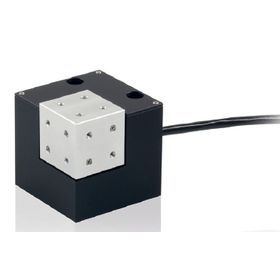
Piezo positioning system
○ Nano control positioning piezo scanner 1 to 6 axes ○ Z-axis piezo scanner for microscopes (PIFOC) ○ Controller ○ Capacitive sensor