iPROS Manufacturing
  • Search for products by classification category

    • Electronic Components and Modules
      Electronic Components and Modules
      56026items
    • Machinery Parts
      Machinery Parts
      70883items
    • Manufacturing and processing machinery
      Manufacturing and processing machinery
      95516items
    • Scientific and Physics Equipment
      Scientific and Physics Equipment
      33048items
    • Materials
      Materials
      34895items
    • Measurement and Analysis
      Measurement and Analysis
      52796items
    • Image Processing
      Image Processing
      14573items
    • Control and Electrical Equipment
      Control and Electrical Equipment
      50342items
    • Tools, consumables, and supplies
      Tools, consumables, and supplies
      62908items
    • Design and production support
      Design and production support
      11724items
    • IT/Network
      IT/Network
      40453items
    • Office
      Office
      13170items
    • Business support services
      Business support services
      32004items
    • Seminars and Skill Development
      Seminars and Skill Development
      5796items
    • Pharmaceutical and food related
      Pharmaceutical and food related
      23523items
    • others
      59606items
  • Search for companies by industry

    • Manufacturing and processing contract
      7353
    • others
      5045
    • Industrial Machinery
      4430
    • Machine elements and parts
      3290
    • Other manufacturing
      2872
    • IT/Telecommunications
      2519
    • Trading company/Wholesale
      2455
    • Industrial Electrical Equipment
      2314
    • Building materials, supplies and fixtures
      1819
    • software
      1648
    • Electronic Components and Semiconductors
      1575
    • Resin/Plastic
      1495
    • Service Industry
      1405
    • Testing, Analysis and Measurement
      1131
    • Ferrous/Non-ferrous metals
      979
    • environment
      701
    • Chemical
      630
    • Automobiles and Transportation Equipment
      560
    • Printing Industry
      506
    • Information and Communications
      434
    • Consumer Electronics
      422
    • Energy
      321
    • Rubber products
      311
    • Food Machinery
      303
    • Optical Instruments
      283
    • robot
      274
    • fiber
      250
    • Paper and pulp
      232
    • Electricity, Gas and Water Industry
      172
    • Pharmaceuticals and Biotechnology
      165
    • Warehousing and transport related industries
      145
    • Glass and clay products
      142
    • Food and Beverage
      134
    • CAD/CAM
      121
    • retail
      110
    • Educational and Research Institutions
      108
    • Medical Devices
      101
    • Ceramics
      96
    • wood
      87
    • Transportation
      83
    • Petroleum and coal products
      61
    • Medical and Welfare
      61
    • Shipbuilding and heavy machinery
      52
    • Aviation & Aerospace
      47
    • Fisheries, Agriculture and Forestry
      39
    • self-employed
      23
    • Public interest/special/independent administrative agency
      22
    • equipment
      19
    • Mining
      17
    • Research and development equipment and devices
      16
    • Materials
      16
    • Government
      14
    • Finance, securities and insurance
      13
    • Individual
      10
    • Restaurants and accommodations
      8
    • cosmetics
      8
    • Police, Fire Department, Self-Defense Forces
      7
    • Laboratory Equipment and Consumables
      3
    • Contracted research
      3
    • Raw materials for reagents and chemicals
      2
  • Special Features
  • Ranking

    • Overall Products Ranking
    • Overall Company Ranking
Search for Products
  • Search for products by classification category

  • Electronic Components and Modules
  • Machinery Parts
  • Manufacturing and processing machinery
  • Scientific and Physics Equipment
  • Materials
  • Measurement and Analysis
  • Image Processing
  • Control and Electrical Equipment
  • Tools, consumables, and supplies
  • Design and production support
  • IT/Network
  • Office
  • Business support services
  • Seminars and Skill Development
  • Pharmaceutical and food related
  • others
Search for Companies
  • Search for companies by industry

  • Manufacturing and processing contract
  • others
  • Industrial Machinery
  • Machine elements and parts
  • Other manufacturing
  • IT/Telecommunications
  • Trading company/Wholesale
  • Industrial Electrical Equipment
  • Building materials, supplies and fixtures
  • software
  • Electronic Components and Semiconductors
  • Resin/Plastic
  • Service Industry
  • Testing, Analysis and Measurement
  • Ferrous/Non-ferrous metals
  • environment
  • Chemical
  • Automobiles and Transportation Equipment
  • Printing Industry
  • Information and Communications
  • Consumer Electronics
  • Energy
  • Rubber products
  • Food Machinery
  • Optical Instruments
  • robot
  • fiber
  • Paper and pulp
  • Electricity, Gas and Water Industry
  • Pharmaceuticals and Biotechnology
  • Warehousing and transport related industries
  • Glass and clay products
  • Food and Beverage
  • CAD/CAM
  • retail
  • Educational and Research Institutions
  • Medical Devices
  • Ceramics
  • wood
  • Transportation
  • Petroleum and coal products
  • Medical and Welfare
  • Shipbuilding and heavy machinery
  • Aviation & Aerospace
  • Fisheries, Agriculture and Forestry
  • self-employed
  • Public interest/special/independent administrative agency
  • equipment
  • Mining
  • Research and development equipment and devices
  • Materials
  • Government
  • Finance, securities and insurance
  • Individual
  • Restaurants and accommodations
  • cosmetics
  • Police, Fire Department, Self-Defense Forces
  • Laboratory Equipment and Consumables
  • Contracted research
  • Raw materials for reagents and chemicals
Special Features
Ranking
  • Overall Products Ranking
  • Overall Company Ranking
  • privacy policy
  • terms of service
  • About Us
  • Careers
  • Advertising
  1. Home
  2. Testing, Analysis and Measurement
  3. 一般財団法人材料科学技術振興財団 MST
  4. Product/Service List
Testing, Analysis and Measurement
  • Added to bookmarks

    Bookmarks list

    Bookmark has been removed

    Bookmarks list

    You can't add any more bookmarks

    By registering as a member, you can increase the number of bookmarks you can save and organize them with labels.

    Free membership registration

一般財団法人材料科学技術振興財団 MST

EstablishmentAugust 1, 1984
addressTokyo/Setagaya-ku/Kitaomi 1-18-6
phone03-3749-2525
  • Special site
  • Official site
last updated:May 26, 2025
一般財団法人材料科学技術振興財団 MSTlogo
  • Contact this company

    Contact Us Online
  • Company information
  • Products/Services(737)
  • catalog(688)
  • news(227)

一般財団法人材料科学技術振興財団 MST List of Products and Services

  • category

1~27 item / All 27 items

Displayed results

Filter by category

Mass spectrometry Mass spectrometry
Photoelectron spectroscopy Photoelectron spectroscopy
[Measurement Method] Electron Microscopy Observation and Analysis [Measurement Method] Electron Microscopy Observation and Analysis
Vibrational spectroscopy Vibrational spectroscopy
Measurement Method: X-ray Diffraction Related Measurement Method: X-ray Diffraction Related
[Measurement Method] Related to SPM [Measurement Method] Related to SPM
Measurement Method: Failure Analysis Measurement Method: Failure Analysis
[Measurement Method] Other Measurement Methods [Measurement Method] Other Measurement Methods
Processing methods and treatment methods Processing methods and treatment methods
Other services and support information Other services and support information
[Analysis Case] LSI・Memory [Analysis Case] LSI・Memory
[Analysis Case] Optical Devices [Analysis Case] Optical Devices
[Analysis Case] Solar Cells [Analysis Case] Solar Cells
[Analysis Case] Fuel Cell [Analysis Case] Fuel Cell
[Analysis Case] Display [Analysis Case] Display
[Analysis Case] Oxide Semiconductors [Analysis Case] Oxide Semiconductors
[Analysis Case] Power Device [Analysis Case] Power Device
[Analysis Case] Electronic Components [Analysis Case] Electronic Components
[Analysis Case] Secondary Battery [Analysis Case] Secondary Battery
[Analysis Case] Lighting [Analysis Case] Lighting
[Analysis Case] Manufacturing Equipment and Components [Analysis Case] Manufacturing Equipment and Components
[Analysis Case] Biotechnology [Analysis Case] Biotechnology
[Analysis Case] Cosmetics [Analysis Case] Cosmetics
[Analysis Case] Food [Analysis Case] Food
[Analysis Case] Pharmaceuticals [Analysis Case] Pharmaceuticals
[Analysis Case] Medical Devices [Analysis Case] Medical Devices
Analysis Case: Daily Necessities Analysis Case: Daily Necessities
[Analysis Case] Environment [Analysis Case] Environment
[Analysis Case] Others [Analysis Case] Others
Materials from the exhibition where MST exhibited. Materials from the exhibition where MST exhibited.
[Measurement

[Measurement Method] Electron Microscopy Observation and Analysis

◆AES (Auger Electron Spectroscopy) ◆SEM (Scanning Electron Microscopy) ◆EBIC (Electron Beam Induced Current) ◆EBSD (Electron Backscatter Diffraction) ◆EDX (Energy Dispersive X-ray Spectroscopy) ◆EPMA (Electron Probe Microanalysis) ◆TEM (Transmission Electron Microscopy) ◆EELS (Electron Energy Loss Spectroscopy) ◆SIM (Scanning Ion Microscopy)

[AES] Auger Electron Spectroscopy

By measuring the kinetic energy distribution of Auger electrons emitted by electron beam irradiation, insights can be gained regarding the types and quantities of elements present on the sample surface.

- Qualitative and quantitative analysis of solid material surfaces (depth of several nm) is possible. - Qualitative and quantitative analysis of micro-regions (approximately tens of nm to sub-micron) is possible. - Depth profile analysis, line analysis, and area analysis of major component elements can be measured. - For several elements such as Si and Al, evaluation in both oxide and metallic states is possible. - Identification of specific areas of interest using SEM images is possible.

Added to bookmarks

Bookmarks list

Bookmark has been removed

Bookmarks list

You can't add any more bookmarks

By registering as a member, you can increase the number of bookmarks you can save and organize them with labels.

Free membership registration

Scanning Electron Microscopy (SEM)

High magnification observation (up to about 300,000 times) is possible.

SEM is a technique that allows for obtaining contrast based on the information from electrons emitted from a sample when an electron beam is directed at it, revealing the sample's surface roughness and compositional differences. - High magnification observation (up to about 500,000 times) is possible with simple operation. - Observation of secondary electron (SE) images, backscattered electron (BSE) images, and transmitted electron (TE) images is possible. - Observation can be conducted within an acceleration voltage range of 0.1 to 30 kV. - Samples up to 6 inches can be loaded into the device (depending on the equipment). - By combining options with SEM, various types of information can be obtained: - Elemental analysis using an EDX detector is possible. - Measurement of electron beam induced current (EBIC) allows for evaluation of the junction position and shape in semiconductors. - Crystal information can be obtained using electron backscatter diffraction (EBSD) method. - Three-dimensional structural information can be acquired through repeated FIB processing and SEM observation (Slice & View). - Cooling observation and atmosphere-controlled observation are available.

Added to bookmarks

Bookmarks list

Bookmark has been removed

Bookmarks list

You can't add any more bookmarks

By registering as a member, you can increase the number of bookmarks you can save and organize them with labels.

Free membership registration

[EBIC] Electron Beam Induced Current

A method to obtain information about the electric field structure inside the sample (junction structure of semiconductors).

By irradiating an electron beam within a SEM device, electron-hole pairs are generated in the sample. Normally, these pairs recombine and disappear, but if they are generated in regions with an internal electric field, such as a depletion layer, the carriers can be drifted by the internal electric field and extracted as a current. This current is referred to as EBIC (Electron Beam Induced Current), and by obtaining it alongside the SEM image, it is possible to visualize the position of the pn junction and the extent of the depletion layer. - Evaluation of pn junctions and crystal defects (dislocations, stacking faults, etc.) is possible. - By overlaying with the SEM image, the positions of the junctions and crystal defects can be identified.

Added to bookmarks

Bookmarks list

Bookmark has been removed

Bookmarks list

You can't add any more bookmarks

By registering as a member, you can increase the number of bookmarks you can save and organize them with labels.

Free membership registration

[EBSD] Electron Backscatter Diffraction Method

It is possible to easily obtain crystal information over a wide area.

This is a method for orientation analysis of crystalline samples using EBSD. It allows for easier and broader acquisition of crystal information compared to electron diffraction methods. EBSP: Electron Backscatter Pattern, also referred to as SEM-OIM or OIM. - Measurement of the surface orientation of single crystal grains is possible. - Orientation measurement of the measurement area is possible. - Observation of crystal grain size is possible. - Observation of twin grain boundaries (corresponding grain boundaries) is possible. - Extraction of specific crystal orientations is possible. - Measurement of the rotation angle of adjacent crystal grains is possible. - Evaluation of grains larger than 10 nm is possible using transmission methods.

Added to bookmarks

Bookmarks list

Bookmark has been removed

Bookmarks list

You can't add any more bookmarks

By registering as a member, you can increase the number of bookmarks you can save and organize them with labels.

Free membership registration

[SEM-EDX] Energy Dispersive X-ray Spectroscopy (SEM)

It is a method for conducting elemental analysis and compositional analysis by detecting characteristic X-rays generated by electron beam irradiation and spectrally analyzing them by energy.

EDX is a method for performing elemental and compositional analysis by detecting characteristic X-rays generated by electron beam irradiation and spectrally analyzing them by energy. It is also referred to as EDS: Energy Dispersive X-ray Spectroscopy. In many cases, it is attached to SEM or TEM, and this document will explain EDX attached to SEM. - The entire energy measurement range (from B to U) can be measured simultaneously in a short time. - It has excellent detection efficiency, allowing measurements with a low probe current. - Analysis can be easily performed without the need for pretreatment, except for special samples. - It is suitable for the analysis of unknown samples. - Measurements can be conducted in a frozen or cooled state using a cryo holder.

Added to bookmarks

Bookmarks list

Bookmark has been removed

Bookmarks list

You can't add any more bookmarks

By registering as a member, you can increase the number of bookmarks you can save and organize them with labels.

Free membership registration

[Slice&View] Three-Dimensional SEM Observation Method

By repeatedly performing cross-sectioning processing with FIB and observation with SEM, and reconstructing the obtained images, three-dimensional structural information can be obtained.

Using a high-resolution SEM device equipped with FIB, we can obtain three-dimensional structural information by repeatedly performing cross-sectioning (Slice) with FIB and observing (View) with SEM, and then reconstructing the acquired images. Similarly, Slice & View is also possible for SIM (Scanning Ion Microscope) images. - It is possible to observe secondary electron (SE), backscattered electron (BSE) images, and scanning ion microscope (SIM) images.

Added to bookmarks

Bookmarks list

Bookmark has been removed

Bookmarks list

You can't add any more bookmarks

By registering as a member, you can increase the number of bookmarks you can save and organize them with labels.

Free membership registration

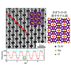
(S)TEM (Scanning Transmission Electron Microscopy)

Elemental analysis, state evaluation, particle size analysis, and acquisition of three-dimensional structural images at the nanoscale.

TEM (Transmission Electron Microscopy) is a method that involves irradiating a thin sample with an electron beam, imaging the electrons that have passed through or scattered from the sample, and observing it at high magnification. ■ Advantages - Enlarged images can be obtained with sub-nanometer spatial resolution, allowing for the observation and analysis of the sample's fine structure and lattice defects. - It is possible to evaluate the crystallinity of the sample and identify materials. - By fabricating samples using FIB (Focused Ion Beam), it is possible to observe specific locations within a device with pinpoint accuracy. - By combining optional features, it is also possible to analyze the composition and state of localized areas. ■ Disadvantages - It is necessary to thin the sample (in some cases, thinning may be difficult for certain samples). - It does not observe individual atoms but rather displays average information in the thickness direction of the sample (typically about 0.1 μm thick). - Sample processing and observation may lead to alteration or deformation of the sample.

Added to bookmarks

Bookmarks list

Bookmark has been removed

Bookmarks list

You can't add any more bookmarks

By registering as a member, you can increase the number of bookmarks you can save and organize them with labels.

Free membership registration

[TEM-EELS] Electron Energy Loss Spectroscopy

By measuring the energy lost due to interactions with atoms as electrons pass through thin film samples, the constituent elements and electronic structure of the material can be analyzed.

EELS analysis is a method that measures the energy lost by electrons as they pass through thin samples due to interactions with atoms. It can analyze the constituent elements and electronic structure of materials. Compared to the elemental analysis device (EDX) attached to a TEM, it has the following features: - Better sensitivity for light elements compared to EDX - Higher energy resolution compared to EDX - Higher spatial resolution compared to EDX, making it difficult to detect surrounding information - Chemical state analysis is possible for certain elements

Added to bookmarks

Bookmarks list

Bookmark has been removed

Bookmarks list

You can't add any more bookmarks

By registering as a member, you can increase the number of bookmarks you can save and organize them with labels.

Free membership registration

[ED] Electron Diffraction Method

ED is a method for investigating crystal structures from diffraction patterns obtained by irradiating a sample with an electron beam.

ED is a method for investigating crystal structures from diffraction patterns obtained by irradiating a sample with an electron beam. - Crystallographic information about the material can be obtained. In the case of a transmission electron microscope, a single crystal shows regularly arranged diffraction spots, a polycrystal shows concentric circular rings, and an amorphous material shows broad circular electron diffraction patterns. - It is possible to examine the crystal structure of small regions observed with a transmission electron microscope. - By combining the crystal structure with elemental analysis results from the EDX method, it is also possible to identify materials that possess crystallinity.

Added to bookmarks

Bookmarks list

Bookmark has been removed

Bookmarks list

You can't add any more bookmarks

By registering as a member, you can increase the number of bookmarks you can save and organize them with labels.

Free membership registration

[SIM] Scanning Ion Microscopy Method

Observation of SIM images is possible with high resolution (accelerating voltage 30kV: 4nm).

- SIM imaging observation is possible with high resolution (accelerating voltage 30kV: 4nm). - Compared to SEM images, SIM images provide information about the extreme surface layer. - Observation of metal crystal grains is possible (e.g., Al, Cu). - The resolution is inferior to SEM images (SIM: 4nm, SEM: 0.5nm). ■Features of MST-owned equipment - Compatible with JEIDA standard wafers with a maximum sample size of 300mm in diameter. - Continuous cross-sectional SIM imaging acquisition is possible in combination with FIB (Focused Ion Beam) processing (Slice & View).

Added to bookmarks

Bookmarks list

Bookmark has been removed

Bookmarks list

You can't add any more bookmarks

By registering as a member, you can increase the number of bookmarks you can save and organize them with labels.

Free membership registration

[TEM-EDX] Energy Dispersive X-ray Spectroscopy (TEM)

EDX is a method that measures the energy and occurrence of characteristic X-rays generated when an electron beam is irradiated onto the analysis area, allowing for elemental analysis and compositional analysis.

EDX is a method that measures the energy and occurrence of characteristic X-rays generated when an electron beam is irradiated onto the analysis target area, allowing for elemental and compositional analysis. It is also referred to as Energy Dispersive X-ray Spectroscopy (EDS). In many cases, it is attached to a SEM or TEM, and this document introduces the EDX that accompanies the TEM. - Simultaneous analysis of the entire range of elements (from B to U) is possible (detection of Be is also possible depending on the attached device). - Measurements can be made with a fine electron beam probe of 0.1 nm in diameter or smaller. - By using drift correction functionality, sub-nanometer layered films can be identified as distribution images in surface analysis. - In surface analysis, it is possible to extract spectra from arbitrary locations and display line analysis.

Added to bookmarks

Bookmarks list

Bookmark has been removed

Bookmarks list

You can't add any more bookmarks

By registering as a member, you can increase the number of bookmarks you can save and organize them with labels.

Free membership registration

[Analysis Case] Degradation Analysis of Liquid Crystal Displays

We will comprehensively evaluate liquid crystals, alignment films, sealing materials, TFTs, and more.

Understanding the degradation mechanism of liquid crystal display panels is an essential theme for extending the lifespan of the panels. Among the degradation symptoms, a decrease in brightness can be attributed to various factors, including liquid crystals, alignment films, sealing materials, and TFTs. A comprehensive analysis will be conducted, incorporating surface, structure, composition, and computational science. By capturing the slight differences between good and defective products and conducting a comprehensive evaluation, we can elucidate the degradation mechanism of liquid crystal displays.

Added to bookmarks

Bookmarks list

Bookmark has been removed

Bookmarks list

You can't add any more bookmarks

By registering as a member, you can increase the number of bookmarks you can save and organize them with labels.

Free membership registration

[Analysis Case] Cell Cycle Assessment from Bacterial Images

By using deep learning and data analysis, we can evaluate sample characteristics by utilizing large amounts of data.

We observed a sample mixed with three types of lactic acid bacteria using SEM, and extracted the bacteria by type using deep learning from the obtained images. Furthermore, we conducted data analysis to determine the presence ratio on the cell cycle based on the shape of the lactic acid bacteria. Measurement methods: SEM, computational science, AI, data analysis Product fields: Biotechnology, pharmaceuticals, daily necessities, cosmetics, food Analysis purpose: Shape evaluation, product investigation For more details, please download the materials or contact us.

Added to bookmarks

Bookmarks list

Bookmark has been removed

Bookmarks list

You can't add any more bookmarks

By registering as a member, you can increase the number of bookmarks you can save and organize them with labels.

Free membership registration

[TEM ED-Map] TEM Electron Diffraction Mapping Method

This is a method for analyzing the orientation distribution of crystalline samples using electron diffraction in a transmission electron microscope (TEM).

By scanning the electron beam probe and measuring the electron diffraction patterns at each point, high spatial resolution crystal information can be obtained. This method allows for the acquisition of information on smaller crystal grains than the EBSD method in SEM. It is also referred to as ACOM (Automated Crystal Orientation Mapping) - TEM method. - Crystal grain size analysis is possible - Orientation measurement of the measurement area is possible - Observation of twin grain boundaries (corresponding grain boundaries) is possible - Extraction of specific crystal orientations is possible - Measurement of the rotation angle of adjacent crystal grains is possible - Evaluation of crystal grains larger than a few nanometers is possible

Added to bookmarks

Bookmarks list

Bookmark has been removed

Bookmarks list

You can't add any more bookmarks

By registering as a member, you can increase the number of bookmarks you can save and organize them with labels.

Free membership registration

[Analysis Case] Evaluation of Two-Dimensional Electron Gas Layer in Normally Off GaN HEMT

We can offer a one-stop solution for comprehensive analysis of product research.

GaN-based high electron mobility transistors, known as GaN HEMTs (High Electron Mobility Transistors), utilize an AlGaN/GaN heterostructure to achieve a two-dimensional electron gas layer (2DEG), resulting in high electron mobility. They are used in applications such as fast chargers, leveraging these characteristics. This document presents the disassembly and evaluation of normally-off GaN HEMT devices. We will introduce a case study that employs a combination of analytical methods to gather comprehensive insights about the samples. Measurement methods: SIMS, TEM, SCM, SMM. Product field: Power devices. Analysis objectives: Trace concentration measurement, shape evaluation, film thickness evaluation, structural evaluation, product investigation. For more details, please download the document or contact us.

Added to bookmarks

Bookmarks list

Bookmark has been removed

Bookmarks list

You can't add any more bookmarks

By registering as a member, you can increase the number of bookmarks you can save and organize them with labels.

Free membership registration

[Analysis Case] Trench-type Si-MOSFET IDSS Leakage Location Analysis

One-stop service from identifying device defects to analyzing causes.

Power devices are attracting attention from the perspective of power and energy conservation as switches for high voltage and large current. In power devices, wiring defects and electrical failures occur due to the application of high voltage. Additionally, identifying and analyzing the causes of defects is essential for improving product reliability. This document presents a case study where the identification of defective areas was conducted using EMS (Emission Microscopy Method), and the analysis of defect causes was evaluated using SCM (Scanning Capacitance Microscopy) and SEM (Scanning Electron Microscopy). Measurement methods: EMS, SCM, SEM Product field: Power devices Analysis purpose: Failure analysis and defect analysis For more details, please download the document or contact us.

Added to bookmarks

Bookmarks list

Bookmark has been removed

Bookmarks list

You can't add any more bookmarks

By registering as a member, you can increase the number of bookmarks you can save and organize them with labels.

Free membership registration

[Analysis Case] Failure Analysis of SiC Transistor using Slice & View

Check the leak path by 3D visualization of SEM images.

For the SiC transistor, where the leak location was identified using a backside emission microscope, cross-sectional SEM observation was conducted using Slice & View. With Slice & View, it is possible to capture images of the leak location without missing it by performing cross-sectional observations at a pitch of several tens of nanometers around the leak area. By converting the SEM images into 3D, the leak path can be confirmed. Measurement method: Slice & View, EMS Product area: Power devices Analysis purpose: Failure analysis, defect analysis, product investigation For more details, please download the materials or contact us.

Added to bookmarks

Bookmarks list

Bookmark has been removed

Bookmarks list

You can't add any more bookmarks

By registering as a member, you can increase the number of bookmarks you can save and organize them with labels.

Free membership registration

[Analysis Case] Component Analysis of Leakage Areas in SiC Power Transistors

It is possible to perform magnified observation and EDX analysis at the gate destruction location identified by Slice & View.

We conducted Slice & View on a SiC transistor where the leak location was identified using a backside emission microscope, and performed magnified observation and SEM-EDX analysis at the confirmed destruction site. Bright contrast was observed in the reflected electron images, indicating the segregation of Si and Ni. It is believed that some segregation of elements such as Si and Ni occurred due to the destruction caused by the leak. Measurement methods: Slice & View, SEM-EDX, EMS Product field: Power devices Analysis purpose: Failure analysis, defect analysis, product investigation For more details, please download the materials or contact us.

Added to bookmarks

Bookmarks list

Bookmark has been removed

Bookmarks list

You can't add any more bookmarks

By registering as a member, you can increase the number of bookmarks you can save and organize them with labels.

Free membership registration

[EPMA] Electron Probe Micro Analyzer

By analyzing the characteristic X-rays generated when a finely focused electron beam is irradiated onto the surface of a solid sample in a vacuum, insights can be gained regarding the identification of elements and quantitative values.

By analyzing characteristic X-rays using a wavelength dispersive X-ray spectrometer (WDX), measurements with higher sensitivity than those obtained with an energy dispersive X-ray spectrometer (EDX) can be achieved. Additionally, using soft X-ray emission spectroscopy (SXES) allows for the acquisition of information regarding local chemical bonding states.

Added to bookmarks

Bookmarks list

Bookmark has been removed

Bookmarks list

You can't add any more bookmarks

By registering as a member, you can increase the number of bookmarks you can save and organize them with labels.

Free membership registration

Identification of resistance anomalies due to absorption current

You can identify high resistance and open areas in the wiring from the absorption current image.

- Possible to identify high resistance abnormal areas - The current flowing through the wiring is weak (pA) - Measurement is possible even with a surface protective film present - Measurement is possible even with multilayered wiring - Measurement is possible under conditions almost identical to SEM observation

Added to bookmarks

Bookmarks list

Bookmark has been removed

Bookmarks list

You can't add any more bookmarks

By registering as a member, you can increase the number of bookmarks you can save and organize them with labels.

Free membership registration

Structural analysis using Xe-plasma FIB.

Precision processing/structural evaluation is possible over a wide area of several hundred micrometers.

It achieves high positional accuracy and wide-area cross-section production, making it usable as a new large-capacity analysis application. Even small structures within a large area can be targeted for processing, enabling wide-area structural analysis.

Added to bookmarks

Bookmarks list

Bookmark has been removed

Bookmarks list

You can't add any more bookmarks

By registering as a member, you can increase the number of bookmarks you can save and organize them with labels.

Free membership registration

[Analysis Case] Lithium-ion Secondary Battery

Accurate evaluation of the separator cross-sectional shape through sample cooling.

The separator, which is a key component material of batteries, influences the characteristics and safety of the battery due to its porosity, shape, and other factors. Currently, mainstream polymer materials such as polyethylene (PE), polypropylene (PP), or their composite materials have low softening points, with PE being around 125°C and PP around 155°C. We will introduce a case where the structure of a PP separator with a low softening point was observed, and cooling was performed during cross-section processing to suppress degradation for evaluation.

Added to bookmarks

Bookmarks list

Bookmark has been removed

Bookmarks list

You can't add any more bookmarks

By registering as a member, you can increase the number of bookmarks you can save and organize them with labels.

Free membership registration

[Analysis Case] STEM, EBSD Image Simulation for Polycrystalline Structure Analysis

Evaluation of crystal forms using simulations.

High-resolution HAADF-STEM images reflect the atomic arrangement of crystals, and by simulating STEM images corresponding to various crystal orientations, they help in accurately understanding the relative orientations between crystal grains and the observed images in polycrystalline materials. This document presents a case where STEM images were simulated from the crystal orientation information obtained by the EBSD method for the crystal grains in a polycrystalline neodymium magnet, and compares them with actual high-resolution HAADF-STEM images.

Added to bookmarks

Bookmarks list

Bookmark has been removed

Bookmarks list

You can't add any more bookmarks

By registering as a member, you can increase the number of bookmarks you can save and organize them with labels.

Free membership registration

[Analysis Case] Analysis of All-Solid-State Batteries

Comprehensive analytical evaluation combining structure, composition, and electrical properties.

Next-generation all-solid-state batteries, which are lithium-ion batteries, are expected to have high safety, high energy density, high output, and a wide operating temperature range. In recent years, research and development aimed at practical application has been actively conducted, but there are various development challenges. At MST, we propose evaluation content suitable for solving development challenges based on comprehensive analysis and evaluation of structure, composition, and electrical properties. This document introduces specific examples of development challenges for all-solid-state batteries, their evaluation content, and representative evaluation methods for each component.

Added to bookmarks

Bookmarks list

Bookmark has been removed

Bookmarks list

You can't add any more bookmarks

By registering as a member, you can increase the number of bookmarks you can save and organize them with labels.

Free membership registration

[Analysis Case] Structural Evaluation of Secondary Battery Separators

Evaluation of the shape and composition of organic/inorganic multilayer structures.

The separator in lithium-ion secondary batteries not only serves the role of isolating the positive and negative electrodes to prevent internal short circuits, but in automotive batteries, it is also required to have heat resistance to prevent a decrease in strength or melting even in high-temperature environments. This report introduces a case study on separators used in overseas automotive batteries, where heat resistance and thermal decomposition behavior were investigated using TG-DTA, and structural and compositional evaluations were conducted using SEM-EDX, FT-IR, XPS, TOF-SIMS, and XRD. It was found that the separator used in the battery consists of a porous polyethylene and a layered structure of polygonal AlO(OH) aimed at heat resistance.

Added to bookmarks

Bookmarks list

Bookmark has been removed

Bookmarks list

You can't add any more bookmarks

By registering as a member, you can increase the number of bookmarks you can save and organize them with labels.

Free membership registration

[Analysis Case] Evaluation of Resistance Values and Li Distribution in Secondary Battery Cathodes

Distribution of resistance values in the electrode cross-section, visualization of conduction paths, and comparison with ion distribution.

The charge and discharge characteristics of lithium-ion secondary batteries are influenced by electronic conductivity. I will introduce a case where the decreased conductivity of active materials, due to degradation or blockage of conduction paths, was visualized as a resistance value distribution using SSRM. By comparing the results obtained from SSRM with the elemental distribution of Li and other elements measured by TOF-SIMS, it is possible to confirm the correlation between resistance values and elemental distribution. Additionally, it is feasible to classify conductive additives and binders based on resistance values, perform statistical processing, and quantify the mixing degree for each material.

Added to bookmarks

Bookmarks list

Bookmark has been removed

Bookmarks list

You can't add any more bookmarks

By registering as a member, you can increase the number of bookmarks you can save and organize them with labels.

Free membership registration

[Analysis Case] Comprehensive Evaluation of Positive Electrode Active Materials in Secondary Batteries

Proposing an evaluation that combines structure, composition, and electricity to solve development issues.

This article introduces a case study evaluating the surface morphology, cross-sectional structure, components, composition, crystal structure, and resistance value distribution of Li(NiCoMn)O2 (NCM), which is used as a positive electrode in lithium-ion secondary batteries. Based on a comprehensive evaluation of structure, composition, and electrical properties, MST proposes assessments suitable for solving development challenges aimed at improving characteristics and enhancing reliability.

Added to bookmarks

Bookmarks list

Bookmark has been removed

Bookmarks list

You can't add any more bookmarks

By registering as a member, you can increase the number of bookmarks you can save and organize them with labels.

Free membership registration
Prev 1 Next
  • 大型品の切削や低コストな複合加工に。ロボットシステムの資料進呈

    大型品の切削や低コストな複合加工に。ロボットシステムの資料進呈

  • イプロスがリアル展示会を主催します! AI/DX 営業・マーケティング展 出展社募集中 リード数・商談数が止まらない!新しいリアル展示会を提供 会期 2026年3月24日(火)~25日(水) 会場 東京ビッグサイト東4ホール 出展概要資料を進呈!
  • 3Dデータ活用WEBセミナー iCAD Technical Fair 10th 人手不足を解消! 設計製造DXの取組 最新3D活用を徹底解説 設計リードタイム1/2!生産性の向上 60日間で実現した2D→3D設計移行 1つのデータを全部門で使い倒す!
    • Contact this company

      Contact Us Online

    Products

    • Search for Products

    Company

    • Search for Companies

    Special Features

    • Special Features

    Ranking

    • Overall Products Ranking
    • Overall Company Ranking

    support

    • site map
    IPROS
    • privacy policy Regarding external transmission of information
    • terms of service
    • About Us
    • Careers
    • Advertising
    COPYRIGHT © 2001-2025 IPROS CORPORATION ALL RIGHTS RESERVED.
    Please note that the English text on this page is automatically translated and may contain inaccuracies.