11/5 Webinar: Basics of Semiconductor Packaging and Quality Control
 CMC RESEARCH Ltd.
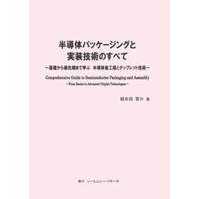
■Title: "Fundamentals of Semiconductor Packaging, Quality Control, and Latest Trends"
――This course systematically explains the functions and structures required for semiconductor packaging, manufacturing processes, and quality control, as well as the latest technological trends such as SiP, WLP, FOWLP, TSV, chipletization, and three-dimensional packaging. Participants will gain an understanding of the overall picture of packaging technology and practical challenges, acquiring the knowledge necessary for semiconductor development and manufacturing.
- Functions required for semiconductor packaging and technological transitions
- Characteristics, challenges, and countermeasures of each subsequent process
- Basic knowledge of package quality control
- Advanced packaging technologies such as SiP, WLP, FOWLP, and TSV
- Latest trends in chipletization and three-dimensional packaging
- Understanding the interrelationship between materials, equipment, and packaging technology
- Young engineers involved in packaging technology
- Engineers from semiconductor equipment manufacturers and material suppliers
- Sales and marketing personnel
- Those who wish to systematically acquire knowledge related to semiconductors
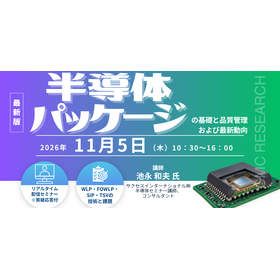
| Date and time | Thursday, Nov 05, 2026 10:30 AM ~ 04:00 PM |
|---|---|
| Entry fee | Charge Participation fee: 55,000 yen (tax included) *Includes materials *For our newsletter members (registration is free) 49,500 yen (tax included) ★If two or more people apply at the same time and all applicants register as newsletter members, the participation fee per person will be half of the newsletter member price. |
Inquiry about this news
Contact Us OnlineMore Details & Registration
Details & Registration
Related product
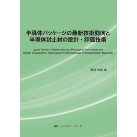
Distributors