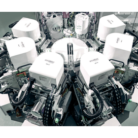
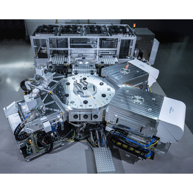
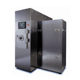
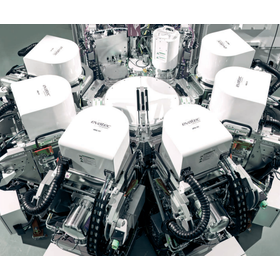
200mm cluster-type sputtering system compatible with thin wafer transport, backside metallization, and piezoelectric materials.
The "CLUSTERLINE 200" is a cluster-type sputtering system designed for 200mm wafers. It features a cluster architecture with cassette-to-cassette processing and fully automated substrate transport. It supports the transport of thin wafers, backside metallization, film formation of new piezoelectric materials such as AlScN, and precision film formation for NIR bandpass filters for consumer devices. Additionally, the new PEALD module for the CLUSTERLINE 200 enables ultra-thin and highly conformal film deposition with atomic-level thickness control, even for complex shapes. *For more details, please feel free to contact us.*
Inquire About This Product
basic information
【Configuration】 ■ Compatible substrate: 200mm wafer ■ Cassette-to-cassette processing with fully automated transport cluster architecture ■ Supports the installation of PEALD modules * For details on configuration and compatible processes, please contact us.
Price range
Delivery Time
Applications/Examples of results
■Thin wafer handling, backside metallization ■Film formation of new piezoelectric materials such as AlScN (wideband RF filters, etc.) ■Precision film formation of NIR bandpass filters for consumer devices ■Ultra-thin, highly conformal films by PEALD
Company information
Evatec's technology has been utilized worldwide for 70 years since the establishment of Balzers AG in 1946. Now, Evatec's thin film manufacturing technology is revolutionizing our lives and ways of working. The Internet of Things (IoT) offers the potential to connect 7 trillion devices for a global population of 7 billion people, and Evatec's thin film manufacturing technology makes this possible. Semiconductor devices manufactured with Evatec's equipment enable millions of people around the world to connect through high-speed wireless networks, changing the way we work due to the evolution of AI. Additionally, autonomous driving made possible by AI semiconductors and high-precision sensing is transforming lifestyles, while power semiconductors allow various devices to operate with less power, addressing energy issues. We provide cutting-edge solutions for thin film manufacturing with high-performance electrical and optical properties, ranging from high-frequency filters essential for wireless communication, high-brightness LEDs for automotive and lighting applications, AI and optoelectronic integrated semiconductors for highly integrated data centers, to touch panels for mobile phones.