
List of Semiconductor Manufacturing Equipment products
- classification:Semiconductor Manufacturing Equipment
46~90 item / All 5194 items


We provide comprehensive support from design to manufacturing and maintenance!


- Contract manufacturing


It won't break even after 1 million repetitions! A mat switch with reliable operation, high durability, and low price. Suitable for options in machine tools as well. Please consult us about delivery t...
- Sensors


Due to its modular embedded design, it is possible to flexibly assemble dedicated machines according to the required film formation methods. A compact thin-film experimental device that can accommodat...
- Sputtering Equipment
- Evaporation Equipment
- Annealing furnace

☆★☆ Spatter and Vapor Deposition Source Combined Film Formation Device 【nanoPVD-ST15A】 ☆★☆
Sputter Cathode and Co-evaporation Source Mixed Thin Film Experimental Device. Metal deposition, organic deposition, and sputter cathode are installed in a compact frame. A resistance heating evaporation source (for metal deposition), an organic evaporation source (for organic materials), and magnetron sputtering (for metals and insulating materials) are installed in the chamber, allowing for various thin film experimental setups within a single chamber. ◉ Three combinations available: 1. Sputter Cathode + Resistance Heating Evaporation Source x2 2. Sputter Cathode + Organic Evaporation Source x2 3. Sputter Cathode + Resistance Heating Source x1 + Organic Evaporation Source x1 (*DC sputtering only) 【Specifications】 ◉ Compatible substrates: up to Φ4 inches ◉ Sputtering: 2" cathode x up to 3 sources ◉ Vacuum deposition: Resistance heating evaporation (up to 2), organic evaporation (up to 4) ◉ 7" touch panel operation with PLC automatic process control ◉ APC automatic pressure control ◉ 1 line of Ar gas (standard) + expandable with N2, O2 ◉ Connects to a Windows PC via USB for recipe creation and storage. Data logging on PC ◉ Various other options available ◉ Easy operation with a 7" touch panel and PLC automatic process control


Visualize surface foreign substances, dirt, and scratches! It is well-received as a daily management tool for yield management, quality control, cleaning management, and hygiene management. *Demo unit...
- Visual Inspection Equipment
- Semiconductor inspection/test equipment
- Defect Inspection Equipment
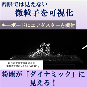
17th High-Performance Materials WEEK [Tokyo] We will be exhibiting a fine particle visualization system at the 17th High-Performance Film Exhibition. (September 30, 2026 (Wed) - October 2, 2026 (Fri) / Makuhari Messe, Hall 2)
The particle visualization technology developed under our brand "ViEST" has a very high level of detection sensitivity that allows for real-time visualization of the suspended and adhered states of micro and nano-sized particles. We are expanding our sales of visualization systems and providing evaluation services (such as investigating particles and airflow in production processes, manufacturing equipment, and factory environments, evaluating the performance of cleaning products, and proposing yield improvement measures) both domestically and internationally. We consistently support the identification of causes and the formulation of countermeasures by visualizing fine foreign substances, particle adhesion due to static electricity, and variations in cleanliness that are problematic in the film manufacturing process. The following are some examples of applications, but by utilizing our technology, we can strongly promote the resolution of various issues such as the deterioration of defect rates caused by fine foreign substances, visualization of clean airflow, and concerns regarding site cleanliness. - Visualization of foreign matter contamination and adhesion mechanisms in the coating and drying processes - Visualization of dust generation and re-adhesion during roll transportation and consideration of countermeasures - Evaluation of airflow and cleanliness within clean booths/clean rooms - Identification of dust sources within manufacturing equipment and promotion of cleanliness - Reduction of foreign matter adhesion risk on film surfaces and improvement of yield


Atomization of liquid without pressurization by piezo vibration. Enables uniform application while reducing power consumption and liquid waste.


- spray
- Coating Machine
- CMP Equipment

Start of distribution of 3D CAD data for Sonia Corporation's ultrasonic spray nozzle.
We have started distributing 3D CAD data for the Sonia ultrasonic spray nozzles. Designers and equipment manufacturers can efficiently proceed with equipment design and layout considerations by confirming product shapes and mounting dimensions in advance. This time, we have also released the 3D CAD data for the ultrasonic spray nozzles "WS40K" and "WS130K," which can be used for interference checks and design simulations before implementation. Sonia's ultrasonic spray nozzles cater to a wide range of applications, including precision coating, surface treatment, humidification, and cleaning. By providing 3D CAD data, we support the reduction of design man-hours and the shortening of development periods, facilitating a smooth process from product selection to equipment development.

Next-generation megasonic technology can instantly clear wafers up to 300mm.
- Photomask
- Other semiconductor manufacturing equipment
- Ultrasonic Cleaner

Our company's handled products, including air nozzles and tank cleaning nozzles from Rehlar, ultrasonic spray nozzles from Sonia, and blowers and air knives (drying devices) from Sonic, have been featured on the industrial product and manufacturer comparison site "Metory."
We are pleased to announce that our company's handled products, including air nozzles from Rehlar, tank cleaning nozzles, ultrasonic spray nozzles from Sonia, and blowers and air knives (drying devices) from Sonic, have been featured on the industrial product and manufacturer comparison site "Metoree." About "Metoree" Metoree is a comparison site for industrial product manufacturers aimed at engineers, researchers, and purchasing professionals. It provides useful information to help engineers easily compare and select products and manufacturers.
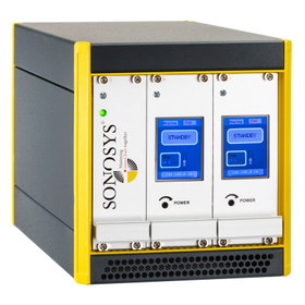
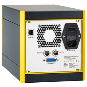
The Digital Generator is a digital control generator compatible with megasonic cleaning systems for semiconductors, electronic components, and precision instruments.
- Photomask
- Other semiconductor manufacturing equipment
- Wafer
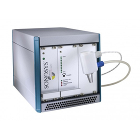
Thorough removal of fine contaminants from wafers. High-quality cleaning achieved by Sonosys.
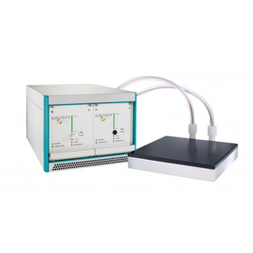
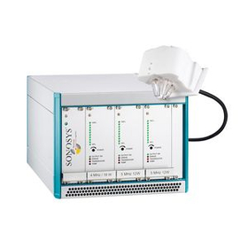
- Ultrasonic Cleaner
- Ultrasonic Oscillator
- Photomask
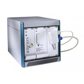
For precise cleaning of prisms. Sonosys ultrasonic cleaning device.
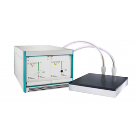
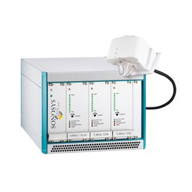
- Ultrasonic Cleaner
- Ultrasonic Oscillator
- Photomask
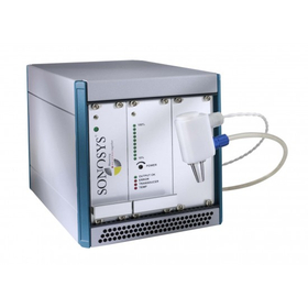
Leave the latest ultrasonic cleaning to Sonosys.


- Photomask
- CMP Equipment
- CVD Equipment
The website of the ultrasonic spray nozzle manufacturer "Sonaer" has been renewed.
The website of the ultrasonic spray nozzle manufacturer "Sonaer" has been renewed. Compared to the previous website, product browsing has improved, and we have also started offering a new system. If you are interested, please feel free to contact us.

Flow spray of 2 mmlit/min or less is possible!
- nozzle
- valve
- Etching Equipment
Start of distribution of 3D CAD data for Sonia Corporation's ultrasonic spray nozzle.
We have started distributing 3D CAD data for the Sonia ultrasonic spray nozzles. Designers and equipment manufacturers can efficiently proceed with equipment design and layout considerations by confirming product shapes and mounting dimensions in advance. This time, we have also released the 3D CAD data for the ultrasonic spray nozzles "WS40K" and "WS130K," which can be used for interference checks and design simulations before implementation. Sonia's ultrasonic spray nozzles cater to a wide range of applications, including precision coating, surface treatment, humidification, and cleaning. By providing 3D CAD data, we support the reduction of design man-hours and the shortening of development periods, facilitating a smooth process from product selection to equipment development.
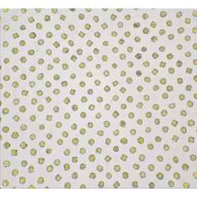

Easy diamond applications. You can trust us with peace of mind.
- Other semiconductors
- Wafer processing/polishing equipment

◉ Short time: Easily conduct graphene synthesis experiments in just 30 minutes per batch. ◉ High-precision temperature and pressure control. ◉ Sophisticated software.
- CVD Equipment
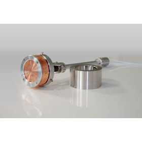
★【Magnetron Sputtering Cathode】★ Thermosera Japan
High-efficiency magnetron sputtering cathode compatible with RF, DC, and pulse DC, capable of depositing metals and insulators without impurities. It also excels in maintainability. 【Features】 - High vacuum compatible - Available in sizes Φ2 inch, Φ3 inch, Φ4 inch - Adopts a clamp ring type, eliminating the need for bonding - Excellent maintainability, allowing for easy target replacement - Rich options including shutters, chimney ports, gas injection, high-strength magnets for magnetic materials, etc. - Compatible with various flange sizes 【Main Specifications】 ■ Compatible with RF, DC, and pulse DC ■ Target thickness: 1/16" to 1/4" ■ N-type coaxial connector ■ Water-cooled: 4ℓ/min, 0.35Mpa Φ6mm tube connection ■ Case material: SUS304 ■ Target clamp material: Al or SUS304 ■ Bellows (*Flexi-head type) material: SUS316 ■ Insulating material: PEEK/PTFE ■ Sealing material: Viton ■ High-strength magnet pack: NiFe

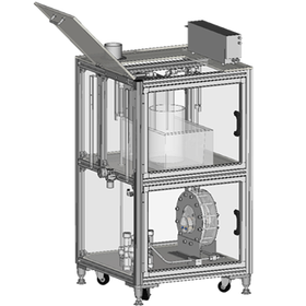
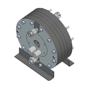
Ion exchange membrane electrolytic cell that achieves both high-purity oxidant production and gas separation.
- Other recycling systems
- Other surface treatment equipment
- Etching Equipment
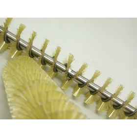

There is a track record of delivering molding equipment. Supporting the cleaning process for semiconductor molds.
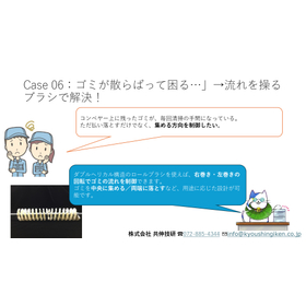
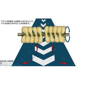
- Conveyor
- Plastic Mould
- Molding Equipment
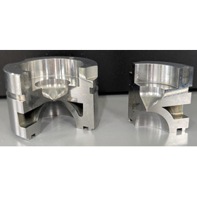

We meet the high precision needs of semiconductor manufacturing with microfabrication and diffusion bonding.
- Special Processing Machinery
- Heat exchanger
- Oxidation/Diffusion Device
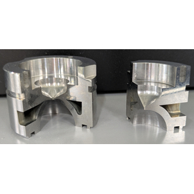
We expand possibilities with microfabrication and diffusion bonding.
- Special Processing Machinery
- Oxidation/Diffusion Device
- Heat exchanger
Joining different materials without melting: A joining technology that balances precision and strength.
- Welding Machine
- Oxidation/Diffusion Device
- Processing Contract
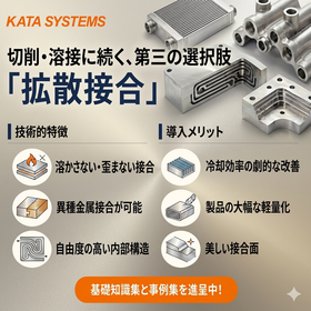
Please use it for demonstration tests and research and development.
- Processing Contract
- Contract manufacturing
- Semiconductor inspection/test equipment
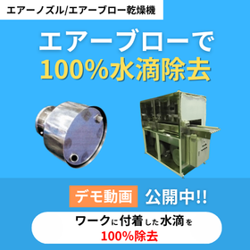

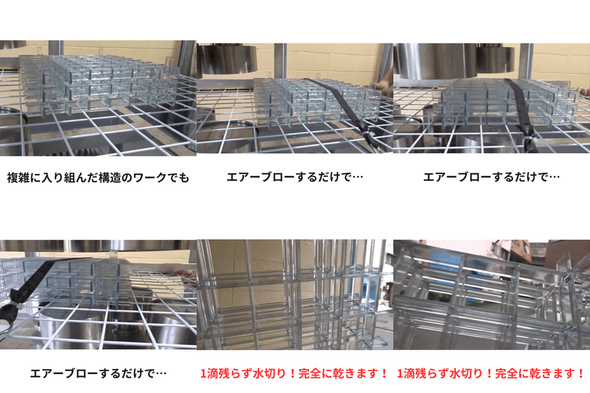
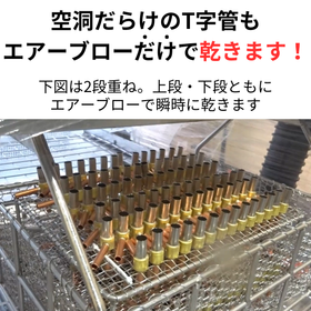
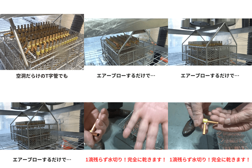
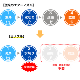
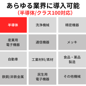
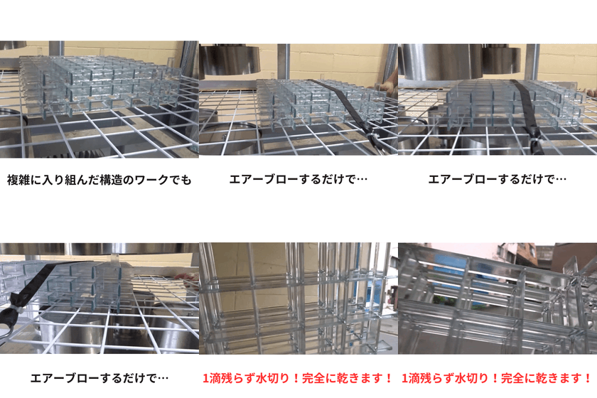
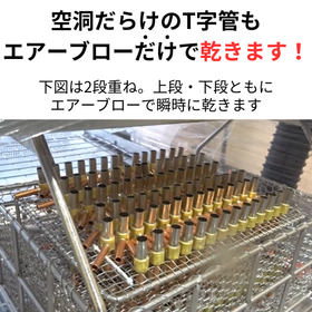
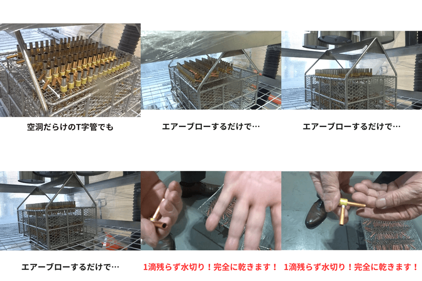
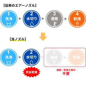
[Patent Obtained] Instant complete water removal of workpieces with air blow = complete drying!
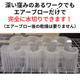
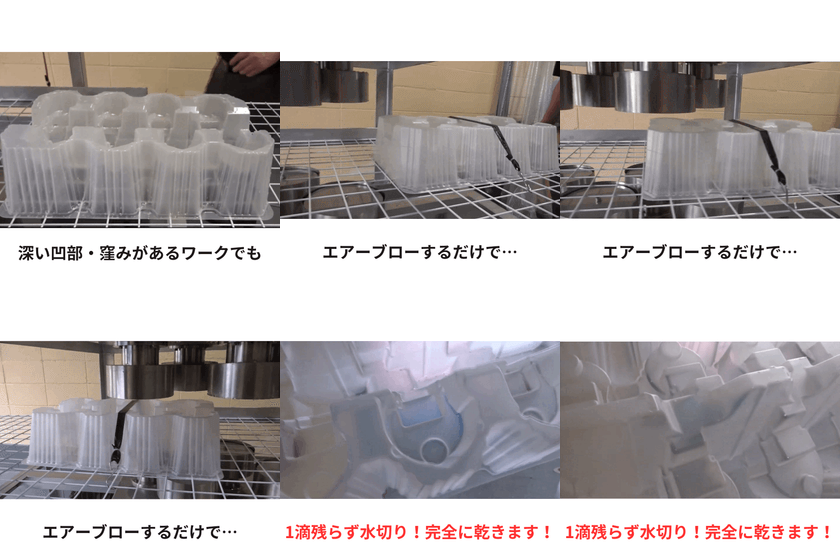
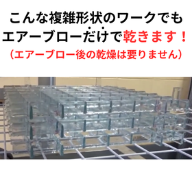

- Other semiconductor manufacturing equipment

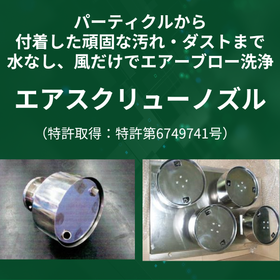
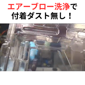
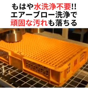
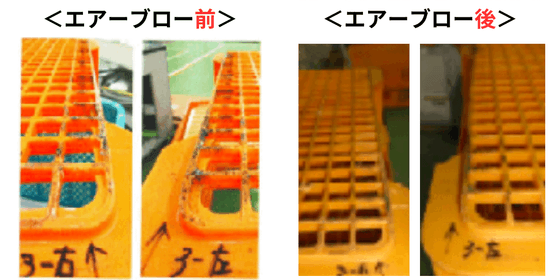
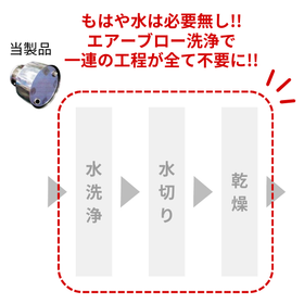
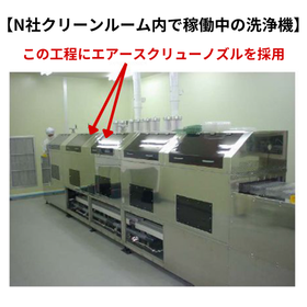
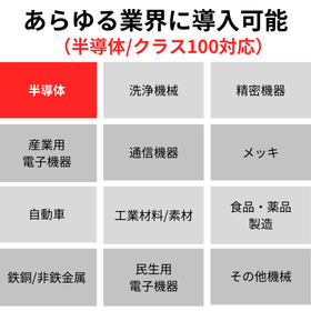
Revolutionary! No need for water washing! Particles are removed with just air blow.

- Other semiconductor manufacturing equipment
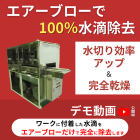
Are you making this mistake when draining water from your work?
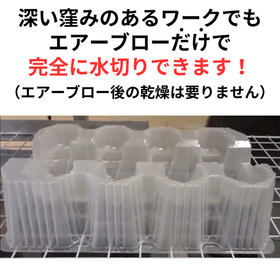
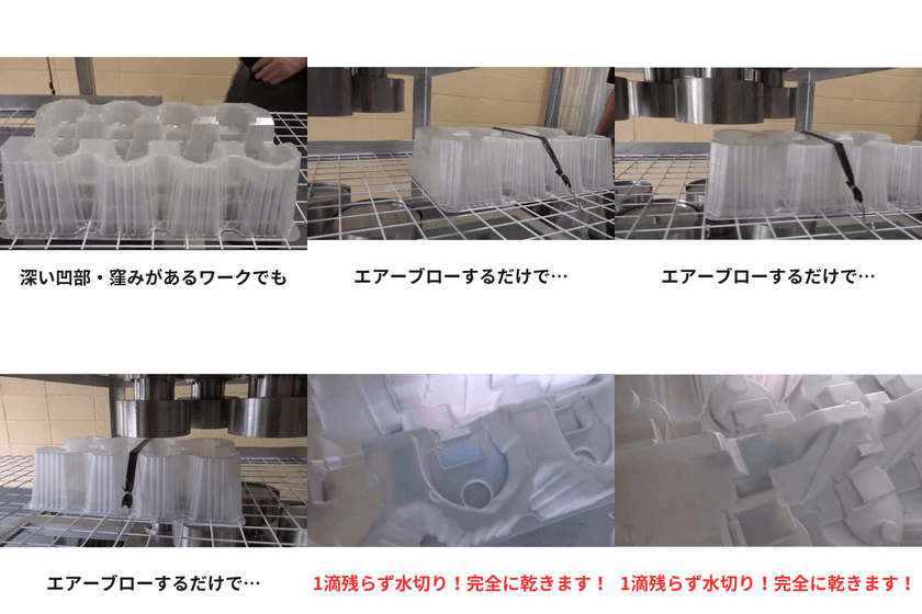
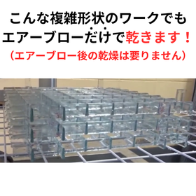

- Other semiconductor manufacturing equipment


Are you making this mistake with the work's drainage?


- Other semiconductor manufacturing equipment

Are you making this mistake while draining water from the work?
[To those in charge who are struggling with workpiece water drainage] Are you making these mistakes with workpiece water drainage? ✓ Do you know the real reason why, even if you increase the air blow pressure, not all water droplets are blown away? ✓ Do you know the real reason why, even if you increase the number of air nozzles, water is not sufficiently drained? ✓ Do you know the real reason why, even if you change the shape of the air nozzle, it still does not drain water effectively? These mistakes are typical errors made by companies that use air blow for workpiece water drainage and droplet removal. However, these mistakes are not significant compared to a certain "fatal mistake." What is that "fatal mistake"? It is… We provide this information in a PDF file. Download it now to find out.

No more revolution! No need for washing; particles are removed with just air blowing.


- Other semiconductor manufacturing equipment

Just by looking at this, you'll understand everything! We created a PR flyer (dust removal version).
Thoroughly remove dust from workpieces with air blow! We have summarized everything about the patented complete dust removal air nozzle, "Air Screw Nozzle," on a single A4 flyer. "What kind of nozzle is it?" "Why can it remove dust so effectively?" "How can it remove dust even from complex-shaped workpieces?" Just by looking at this, you can quickly understand everything about the Air Screw Nozzle. Please download and take a look.

[Patent Obtained] Complete water removal in an instant with air blow = complete drying!


- Other semiconductor manufacturing equipment

If you see this, you'll understand everything! I created a PR flyer.
100% water removal with air blow! No water droplets left on the workpiece! We have summarized everything about the patented complete drying air nozzle, "Air Screw Nozzle," on a single A4 flyer. "What kind of nozzle is it?" "Can it really remove 100% of the water?" "Why is it so effective at removing water?" Just by looking at this, you can quickly understand everything about the Air Screw Nozzle. Please download it and take a look!


Total solution provided from equipment development stage to line operation! Operates stably in a light noise environment.
- Other semiconductor manufacturing equipment

We will solve the shortage of outsourcing partners for precision processing due to capacity overload at existing factories, such as in semiconductors and precision components.
- Etching Equipment

It excels in high sensitivity detection, quantification, and portability, making it suitable for quality inspection and research and development settings. It contributes to the detection of minute for...
- Semiconductor inspection/test equipment
- Other Sanitation Inspections
- Other appearance and image inspection equipment
17th High-Performance Materials WEEK [Tokyo] We will be exhibiting a fine particle visualization system at the 17th High-Performance Film Exhibition. (September 30, 2026 (Wed) - October 2, 2026 (Fri) / Makuhari Messe, Hall 2)
The particle visualization technology developed under our brand "ViEST" has a very high level of detection sensitivity that allows for real-time visualization of the suspended and adhered states of micro and nano-sized particles. We are expanding our sales of visualization systems and providing evaluation services (such as investigating particles and airflow in production processes, manufacturing equipment, and factory environments, evaluating the performance of cleaning products, and proposing yield improvement measures) both domestically and internationally. We consistently support the identification of causes and the formulation of countermeasures by visualizing fine foreign substances, particle adhesion due to static electricity, and variations in cleanliness that are problematic in the film manufacturing process. The following are some examples of applications, but by utilizing our technology, we can strongly promote the resolution of various issues such as the deterioration of defect rates caused by fine foreign substances, visualization of clean airflow, and concerns regarding site cleanliness. - Visualization of foreign matter contamination and adhesion mechanisms in the coating and drying processes - Visualization of dust generation and re-adhesion during roll transportation and consideration of countermeasures - Evaluation of airflow and cleanliness within clean booths/clean rooms - Identification of dust sources within manufacturing equipment and promotion of cleanliness - Reduction of foreign matter adhesion risk on film surfaces and improvement of yield


I will explain in detail the differences between Teflon and fluoropolymer, which are often confused.


- Other semiconductor manufacturing equipment

"We want to confirm the effectiveness of the coating in advance." To meet such needs, Yoshida SKT also offers measurements of the coated surface.
- Resist Device

[Presentation of Materials] We will introduce the differences in features between Teflon fluoropolymer "PTFE" and "PFA" resins and coatings.


- Other semiconductor manufacturing equipment

I will explain the differences between fluororesin and Teflon.


- Other semiconductor manufacturing equipment
Control metal ion contamination at the ppb level. Protect high-purity processes with fluororesin.
- Other semiconductor manufacturing equipment
Eliminate particle and ESD defects caused by static electricity. Unique coating that achieves both static prevention and non-stick properties.
- others
- Other semiconductor manufacturing equipment
From preventing scratches and chips on the transport handle to measures against corrosion of the structure. Coatings that enhance the reliability of wafer transport.
- Other semiconductor manufacturing equipment
Corrosion prevention, prevention of metal ion leaching, and prevention of wafer scratches. Summarizing and solving the challenges of cleaning equipment.
- Other semiconductor manufacturing equipment
Easily removes contaminants with low surface energy. A coating that significantly improves maintainability.
- Other semiconductor manufacturing equipment
Resistant to strong acids, strong alkalis, and organic solvents. A chemical-resistant coating compatible with all processes in semiconductor manufacturing.
- Other semiconductor manufacturing equipment
Prevent damage, adhesion, and metal powder generation on wafers, and maintain a clean environment in the inspection process.
- Other semiconductor manufacturing equipment
Chemical stability that withstands various chemical environments. An optimal fluororesin coating for corrosion prevention in semiconductor manufacturing equipment.
- Other semiconductor manufacturing equipment