
List of Semiconductors and ICs products
- classification:Semiconductors and ICs
766~810 item / All 4837 items


It won't break even after 1 million repetitions! A mat switch with reliable operation, high durability, and low price. Suitable for options in machine tools as well. Please consult us about delivery t...
- Sensors


We can accommodate high resistance over 10,000 ohms, with diameters ranging from approximately 30 mm to 8 inches, and we also offer thinning and chip processing arrangements!
- Other semiconductors
- Processing Contract
- Wafer


A device that changes the "quality" of circulating water and removes scale by performing special electrolysis on the circulating water without using chemical agents.
- Other semiconductors

High-performance aluminum structural materials that meet all the needs of FA, from LCD and semiconductor equipment to various industrial machinery.
- Other semiconductors

High heat resistance: SX-200 can be used continuously at 400°C! Radiation resistance: over 109 RAD.
- Other semiconductors

Further pursuit of lightweight and compact design. The inner diameter of the tube ranges from φ2.5 to φ250, allowing for a wide variety of uses from simple applications to more advanced ones.
- Other semiconductors

Equipped with a slow start, slow stop mechanism, speed controller, digital timer minimizer, and a linkage system for automatic spraying devices, etc.
- Other semiconductors

We guarantee consistently stable wraps and promise a magnificent mirror finish.
- Other semiconductors

Extremely uniform with minimal lot variation.
- Other semiconductors

It is a resin that can be cured in a short time by exposing it to ultraviolet light with a wavelength of 200 to 400 nm.
- Other semiconductors

PEEK is a thermoplastic super heat-resistant resin that combines excellent mechanical properties and functionality.
- Other semiconductors

Excellent corrosion resistance (e.g., hundreds of times that of stainless steel in the case of concentrated hydrochloric acid)
- Other semiconductors

It is an abrasive with strong crushing strength and thermal stability.
- Other semiconductors

A lineup of 5 types of grain sizes.
- Other semiconductors

As of April 1, 2016, the old product name YUPIMORE(R) has been changed to SEPLAS SA.


- Other semiconductors


We have assembled equipment that is strong in the analysis of organic materials such as resin and carbon composites.
- diode
- Contract measurement
- Composite Materials

Announcement of the Start of Non-Destructive Testing Services from April 2018
On April 2, 2018, MST will introduce the latest processing and analysis equipment and begin offering non-destructive analysis services. We will provide analysis services across a wide range of fields, including product development and quality control in electronic devices, pharmaceuticals, and food. Non-destructive analysis is a technology that visualizes the internal condition of a product without destroying it. With the introduction of the latest processing and analysis equipment, MST will now be able to conduct non-destructive analysis. We will offer analysis services on a contract basis.

GC/MS: Gas Chromatography-Mass Spectrometry
- Contract Analysis
- Memory

AFM: Atomic Force Microscopy Method
- Contract Analysis
- Wafer
![[Analysis Case] De-gassing Evaluati...](https://image.mono.ipros.com/public/product/image/d53/2000428729/IPROS15215178984570750876.jpg?w=280&h=280)
You can investigate the changes in degassing intensity while maintaining the temperature.
- Contract Analysis
- Memory
![[Analysis Case] High Sensitivity Ev...](https://image.mono.ipros.com/public/product/image/f9d/2000432944/IPROS14229396913645536742.jpg?w=280&h=280)
The diffusion layer structure of SiC devices can be visualized (high-sensitivity evaluation of the diffusion layer structure).
- Contract Analysis
- Transistor
![[Analysis Case] STEM/EDX and Image ...](https://image.mono.ipros.com/public/product/image/1ac/2000436264/IPROS14066786507828876230.jpg?w=280&h=280)
The evaluation of the crystal structure can be performed based on the STEM images and the results of atomic composition measurements.
- Contract Analysis
- magnet
- Memory
![[Analysis Case] Structural Analysis...](https://image.mono.ipros.com/public/product/image/464/2000437277/IPROS86695334060655697793.jpeg?w=280&h=280)
Microscopic structural analysis of amorphous films is possible through simulation.
- Contract Analysis
- Memory
![[Analysis Case] Stress Evaluation b...](https://image.mono.ipros.com/public/product/image/36f/2000428854/IPROS12617040219046789948.jpg?w=280&h=280)
It is possible to confirm the stress distribution in the sample cross-section.
- Contract Analysis
- Wafer
![[Analysis Case] Valence Evaluation ...](https://image.mono.ipros.com/public/product/image/ea0/2000428856/IPROS8446518364754696871.jpg?w=280&h=280)
It is possible to evaluate trace metals in ppm orders.
- Contract Analysis
- Ceramics
- Wafer
![[Analysis Case] Evaluation of Funct...](https://image.mono.ipros.com/public/product/image/aad/2000428954/IPROS18012351899549271165.jpg?w=280&h=280)
Evaluation of functional groups in graphene is possible using thermal decomposition GC/MS method.
- Contract Analysis
- Transistor
- Power storage device
![[Analysis Case] Non-destructive 3D ...](https://image.mono.ipros.com/public/product/image/507/2000436241/IPROS15768870373445412704.jpg?w=280&h=280)
Non-destructive three-dimensional observation of the internal structure of a discrete package.


- Contract Analysis
- Other semiconductors
![[Analysis Case] Evaluation of Surfa...](https://image.mono.ipros.com/public/product/image/ba3/2000436245/IPROS14534065085904199956.jpg?w=280&h=280)
Quantitative evaluation of the roughness of trench sidewalls related to device characteristics.
- Contract Analysis
- Other semiconductors
![[Analysis Case] Electronic State Ev...](https://image.mono.ipros.com/public/product/image/fc4/2000442424/IPROS92815948388030927297.jpeg?w=280&h=280)
Evaluation of microscopic atomic structures is possible through computational simulation.
- Contract Analysis
- Other semiconductors
![[Analysis Case] Structural Analysis...](https://image.mono.ipros.com/public/product/image/4af/2000442428/IPROS10654005163802715970.jpg?w=280&h=280)
Reverse engineering of DRAM on the product's internal substrate.
- Contract Analysis
- Memory
![[Analysis Case] Observation of Crys...](https://image.mono.ipros.com/public/product/image/a23/2000442436/IPROS15295605371207538123.jpg?w=280&h=280)
It is possible to obtain insights into the size and distribution of crystal grains in metallic polycrystals.
- Contract Analysis
- Memory
![[Analysis Case] Depth Direction Ana...](https://image.mono.ipros.com/public/product/image/e89/2001523596/IPROS13835893106959613763.jpg?w=280&h=280)
It is possible to capture molecular information of inorganic substances in the depth direction using TOF-SIMS.


- Contract measurement
- Transistor
- Memory
![[Analysis Case] Simultaneous Qualit...](https://image.mono.ipros.com/public/product/image/c6d/2001528047/IPROS16763775033636229157.jpg?w=280&h=280)
Simultaneous measurement of inorganic and organic components in minute specific areas.


- Contract measurement
- Wafer
- Memory
![[Analysis Case] Evaluation of Inter...](https://image.mono.ipros.com/public/product/image/64b/2000443018/IPROS11040675799948172833.jpg?w=280&h=280)
We evaluate abnormalities inside the device non-destructively.
- Contract Analysis
- Other electronic parts
- Transistor
![[Analysis Case] Evaluation of Metal...](https://image.mono.ipros.com/public/product/image/19d/2001538620/IPROS12249256516974712398.jpg?w=280&h=280)
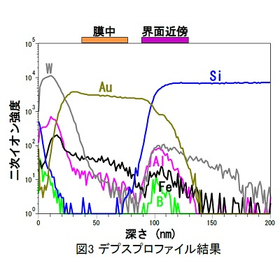
Impurities in films and interfaces such as plating can be evaluated using TOF-SIMS.
- Wafer
- Contract measurement
- Other semiconductors
![[Analysis Case] Composition Analysi...](https://image.mono.ipros.com/public/default/object/noimage_l.gif?w=280&h=280)
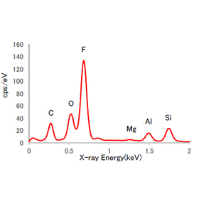
Shape observation and simple quantitative analysis using SEM-EDX.
- Contract Inspection
- Wafer
- Other semiconductor manufacturing equipment
![[Analysis Case] Comparison of Secon...](https://image.mono.ipros.com/public/product/image/b04/2000442432/IPROS8264588846146999573.jpg?w=280&h=280)
It is effective to differentiate between the two methods depending on the surface structure of interest.
- Contract Analysis
- Memory

High-sensitivity analysis of various solutions, such as pure water and wafer cleaning liquids, is possible.
- Contract Analysis
- Wafer
- Water quality testing
![[Analysis Case] Competitive Adsorpt...](https://image.mono.ipros.com/public/product/image/387108/IPROS9160298122875376108.jpg?w=280&h=280)
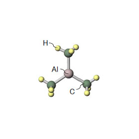
It is possible to evaluate the competitive adsorption of multiple molecules using the focus parameters for film formation (temperature, pressure).
- Contract Analysis
- Other electronic parts
- Memory
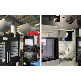

From semiconductor and LCD manufacturing equipment parts to nursing and welfare equipment parts. MINWA delivers high-precision and high-quality machining.
- Other semiconductors
- LCD display
- Other machine elements
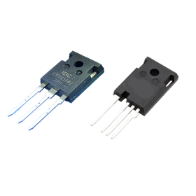

The introduction of the laminated substrate reduces the degradation of the forward characteristics of the body diode!
- diode
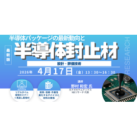

The encapsulating materials for advanced semiconductor packages require various characteristics such as low stress, moisture resistance, and high reliability. Guidelines for the design and evaluation ...
- Other semiconductors
- Engineering Plastics
- Technical Seminar
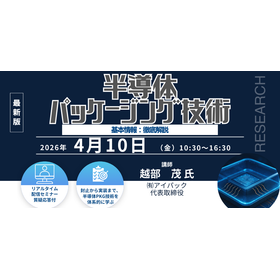
A systematic explanation from the basics of semiconductor packaging to the design and evaluation of encapsulation materials. Leading experts thoroughly organize practical perspectives from WLP/PLP to ...
- Other semiconductor manufacturing equipment
- Other semiconductors
- Technical Seminar
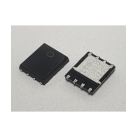
Achieve high current while minimizing losses during implementation with Power PKG (HSOP8)!
- Transistor
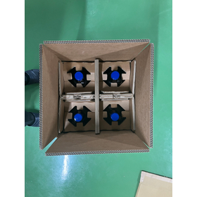

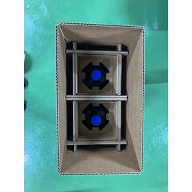
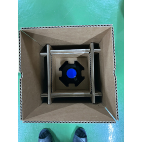
Liquid hazardous materials can also be safely transported with all-fiber solutions.
- Wafer
- Resist Device
- Photomask
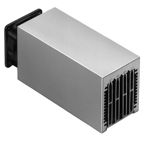

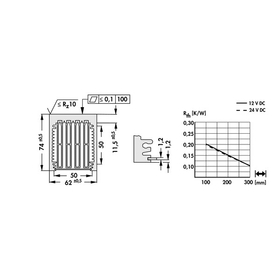
For thermal management of medium-sized devices. You can specify the ideal length in 1mm increments, without being constrained by the fixed sizes in the catalog, to match the enclosure space.
- Other semiconductors