List of Semiconductors and ICs products

  • classification:Semiconductors and ICs

631~675 item / All 4814 items

Displayed results

Reduce the workload from handling heavy objects! Here are five case studies that solved customer challenges! We are also accepting free consultations and tests tailored to your work!

  • PRエリア.png
  • Other conveying machines

Added to bookmarks

Bookmarks list

Bookmark has been removed

Bookmarks list

You can't add any more bookmarks

By registering as a member, you can increase the number of bookmarks you can save and organize them with labels.

Free membership registration

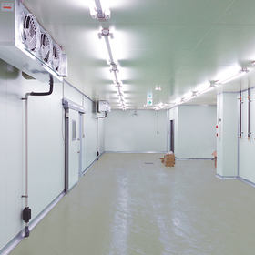
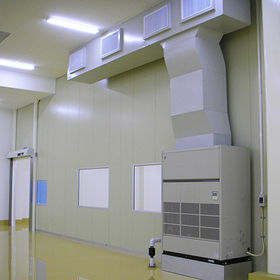
Strong cold wind from room temperature to -13°C! Depending on the usage environment, you can choose between the combo type or the separate type!

  • Cooling system

Added to bookmarks

Bookmarks list

Bookmark has been removed

Bookmarks list

You can't add any more bookmarks

By registering as a member, you can increase the number of bookmarks you can save and organize them with labels.

Free membership registration
image_66.png

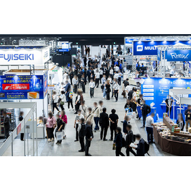
April 10, 2024 (Wednesday) to April 12, 2024 (Friday) Notice of Participation in Nagoya Manufacturing World 2024

Sanwa Shiki Ventilator Co., Ltd. will be exhibiting at the 2024 Monozukuri World (Nagoya) held at Port Messe Nagoya. We will also be showcasing our large cooling fans and cool/warm ambient products. Date: April 10, 2024 - April 12, 2024 Opening: 10:00 AM Location: Nagoya Port Messe (Exhibition Hall 1) *Our booth: 19-1 We would be grateful if you could visit us if you have the time.

We guarantee consistently stable wraps and promise a magnificent mirror finish.

  • Other semiconductors

Added to bookmarks

Bookmarks list

Bookmark has been removed

Bookmarks list

You can't add any more bookmarks

By registering as a member, you can increase the number of bookmarks you can save and organize them with labels.

Free membership registration

Extremely uniform with minimal lot variation.

  • Other semiconductors

Added to bookmarks

Bookmarks list

Bookmark has been removed

Bookmarks list

You can't add any more bookmarks

By registering as a member, you can increase the number of bookmarks you can save and organize them with labels.

Free membership registration

It is a resin that can be cured in a short time by exposing it to ultraviolet light with a wavelength of 200 to 400 nm.

  • Other semiconductors

Added to bookmarks

Bookmarks list

Bookmark has been removed

Bookmarks list

You can't add any more bookmarks

By registering as a member, you can increase the number of bookmarks you can save and organize them with labels.

Free membership registration

PEEK is a thermoplastic super heat-resistant resin that combines excellent mechanical properties and functionality.

  • Other semiconductors

Added to bookmarks

Bookmarks list

Bookmark has been removed

Bookmarks list

You can't add any more bookmarks

By registering as a member, you can increase the number of bookmarks you can save and organize them with labels.

Free membership registration

Excellent corrosion resistance (e.g., hundreds of times that of stainless steel in the case of concentrated hydrochloric acid)

  • Other semiconductors

Added to bookmarks

Bookmarks list

Bookmark has been removed

Bookmarks list

You can't add any more bookmarks

By registering as a member, you can increase the number of bookmarks you can save and organize them with labels.

Free membership registration

It is an abrasive with strong crushing strength and thermal stability.

  • Other semiconductors

Added to bookmarks

Bookmarks list

Bookmark has been removed

Bookmarks list

You can't add any more bookmarks

By registering as a member, you can increase the number of bookmarks you can save and organize them with labels.

Free membership registration

A lineup of 5 types of grain sizes.

  • Other semiconductors

Added to bookmarks

Bookmarks list

Bookmark has been removed

Bookmarks list

You can't add any more bookmarks

By registering as a member, you can increase the number of bookmarks you can save and organize them with labels.

Free membership registration

As of April 1, 2016, the old product name YUPIMORE(R) has been changed to SEPLAS SA.

  • SA101板.jpg
  • SA201板.jpg
  • Other semiconductors

Added to bookmarks

Bookmarks list

Bookmark has been removed

Bookmarks list

You can't add any more bookmarks

By registering as a member, you can increase the number of bookmarks you can save and organize them with labels.

Free membership registration

We have assembled equipment that is strong in the analysis of organic materials such as resin and carbon composites.

  • diode
  • Contract measurement
  • Composite Materials

Added to bookmarks

Bookmarks list

Bookmark has been removed

Bookmarks list

You can't add any more bookmarks

By registering as a member, you can increase the number of bookmarks you can save and organize them with labels.

Free membership registration
hihakai_img.jpg

Announcement of the Start of Non-Destructive Testing Services from April 2018

On April 2, 2018, MST will introduce the latest processing and analysis equipment and begin offering non-destructive analysis services. We will provide analysis services across a wide range of fields, including product development and quality control in electronic devices, pharmaceuticals, and food. Non-destructive analysis is a technology that visualizes the internal condition of a product without destroying it. With the introduction of the latest processing and analysis equipment, MST will now be able to conduct non-destructive analysis. We will offer analysis services on a contract basis.

Added to bookmarks

Bookmarks list

Bookmark has been removed

Bookmarks list

You can't add any more bookmarks

By registering as a member, you can increase the number of bookmarks you can save and organize them with labels.

Free membership registration

Added to bookmarks

Bookmarks list

Bookmark has been removed

Bookmarks list

You can't add any more bookmarks

By registering as a member, you can increase the number of bookmarks you can save and organize them with labels.

Free membership registration

You can investigate the changes in degassing intensity while maintaining the temperature.

  • Contract Analysis
  • Memory

Added to bookmarks

Bookmarks list

Bookmark has been removed

Bookmarks list

You can't add any more bookmarks

By registering as a member, you can increase the number of bookmarks you can save and organize them with labels.

Free membership registration

The diffusion layer structure of SiC devices can be visualized (high-sensitivity evaluation of the diffusion layer structure).

  • Contract Analysis
  • Transistor

Added to bookmarks

Bookmarks list

Bookmark has been removed

Bookmarks list

You can't add any more bookmarks

By registering as a member, you can increase the number of bookmarks you can save and organize them with labels.

Free membership registration

The evaluation of the crystal structure can be performed based on the STEM images and the results of atomic composition measurements.

  • Contract Analysis
  • magnet
  • Memory

Added to bookmarks

Bookmarks list

Bookmark has been removed

Bookmarks list

You can't add any more bookmarks

By registering as a member, you can increase the number of bookmarks you can save and organize them with labels.

Free membership registration

Microscopic structural analysis of amorphous films is possible through simulation.

  • Contract Analysis
  • Memory

Added to bookmarks

Bookmarks list

Bookmark has been removed

Bookmarks list

You can't add any more bookmarks

By registering as a member, you can increase the number of bookmarks you can save and organize them with labels.

Free membership registration

It is possible to confirm the stress distribution in the sample cross-section.

  • Contract Analysis
  • Wafer

Added to bookmarks

Bookmarks list

Bookmark has been removed

Bookmarks list

You can't add any more bookmarks

By registering as a member, you can increase the number of bookmarks you can save and organize them with labels.

Free membership registration

It is possible to evaluate trace metals in ppm orders.

  • Contract Analysis
  • Ceramics
  • Wafer

Added to bookmarks

Bookmarks list

Bookmark has been removed

Bookmarks list

You can't add any more bookmarks

By registering as a member, you can increase the number of bookmarks you can save and organize them with labels.

Free membership registration

Evaluation of functional groups in graphene is possible using thermal decomposition GC/MS method.

  • Contract Analysis
  • Transistor
  • Power storage device

Added to bookmarks

Bookmarks list

Bookmark has been removed

Bookmarks list

You can't add any more bookmarks

By registering as a member, you can increase the number of bookmarks you can save and organize them with labels.

Free membership registration

Non-destructive three-dimensional observation of the internal structure of a discrete package.

  • サンプル内部構造.png
  • サンプル全景.png
  • サンプル外観.png
  • X線透過像.png
  • 開封後のサンプル内部構造.png
  • Contract Analysis
  • Other semiconductors

Added to bookmarks

Bookmarks list

Bookmark has been removed

Bookmarks list

You can't add any more bookmarks

By registering as a member, you can increase the number of bookmarks you can save and organize them with labels.

Free membership registration

Quantitative evaluation of the roughness of trench sidewalls related to device characteristics.

  • Contract Analysis
  • Other semiconductors

Added to bookmarks

Bookmarks list

Bookmark has been removed

Bookmarks list

You can't add any more bookmarks

By registering as a member, you can increase the number of bookmarks you can save and organize them with labels.

Free membership registration

Evaluation of microscopic atomic structures is possible through computational simulation.

  • Contract Analysis
  • Other semiconductors

Added to bookmarks

Bookmarks list

Bookmark has been removed

Bookmarks list

You can't add any more bookmarks

By registering as a member, you can increase the number of bookmarks you can save and organize them with labels.

Free membership registration

Reverse engineering of DRAM on the product's internal substrate.

  • Contract Analysis
  • Memory

Added to bookmarks

Bookmarks list

Bookmark has been removed

Bookmarks list

You can't add any more bookmarks

By registering as a member, you can increase the number of bookmarks you can save and organize them with labels.

Free membership registration

It is possible to obtain insights into the size and distribution of crystal grains in metallic polycrystals.

  • Contract Analysis
  • Memory

Added to bookmarks

Bookmarks list

Bookmark has been removed

Bookmarks list

You can't add any more bookmarks

By registering as a member, you can increase the number of bookmarks you can save and organize them with labels.

Free membership registration

It is possible to capture molecular information of inorganic substances in the depth direction using TOF-SIMS.

  • img_C0264_2.jpg
  • img_C0264_3_HO-Si-O.jpg
  • img_C0264_4_O-Si-O-Si-O.jpg
  • img_C0264_5_Si-N-Si.jpg
  • img_C0264_6_Si-Si.jpg
  • Contract measurement
  • Transistor
  • Memory

Added to bookmarks

Bookmarks list

Bookmark has been removed

Bookmarks list

You can't add any more bookmarks

By registering as a member, you can increase the number of bookmarks you can save and organize them with labels.

Free membership registration

Simultaneous measurement of inorganic and organic components in minute specific areas.

  • img_C0034_4.jpg
  • img_C0034_5.jpg
  • img_C0034_6.jpg
  • Contract measurement
  • Wafer
  • Memory

Added to bookmarks

Bookmarks list

Bookmark has been removed

Bookmarks list

You can't add any more bookmarks

By registering as a member, you can increase the number of bookmarks you can save and organize them with labels.

Free membership registration

We evaluate abnormalities inside the device non-destructively.

  • Contract Analysis
  • Other electronic parts
  • Transistor

Added to bookmarks

Bookmarks list

Bookmark has been removed

Bookmarks list

You can't add any more bookmarks

By registering as a member, you can increase the number of bookmarks you can save and organize them with labels.

Free membership registration

Impurities in films and interfaces such as plating can be evaluated using TOF-SIMS.

  • img_c0638_2.jpg
  • Wafer
  • Contract measurement
  • Other semiconductors

Added to bookmarks

Bookmarks list

Bookmark has been removed

Bookmarks list

You can't add any more bookmarks

By registering as a member, you can increase the number of bookmarks you can save and organize them with labels.

Free membership registration

Shape observation and simple quantitative analysis using SEM-EDX.

  • img_C0736_2.jpg
  • Contract Inspection
  • Wafer
  • Other semiconductor manufacturing equipment

Added to bookmarks

Bookmarks list

Bookmark has been removed

Bookmarks list

You can't add any more bookmarks

By registering as a member, you can increase the number of bookmarks you can save and organize them with labels.

Free membership registration

It is effective to differentiate between the two methods depending on the surface structure of interest.

  • Contract Analysis
  • Memory

Added to bookmarks

Bookmarks list

Bookmark has been removed

Bookmarks list

You can't add any more bookmarks

By registering as a member, you can increase the number of bookmarks you can save and organize them with labels.

Free membership registration

High-sensitivity analysis of various solutions, such as pure water and wafer cleaning liquids, is possible.

  • Contract Analysis
  • Wafer
  • Water quality testing

Added to bookmarks

Bookmarks list

Bookmark has been removed

Bookmarks list

You can't add any more bookmarks

By registering as a member, you can increase the number of bookmarks you can save and organize them with labels.

Free membership registration

It is possible to evaluate the competitive adsorption of multiple molecules using the focus parameters for film formation (temperature, pressure).

  • img_C0743_3.jpg
  • Contract Analysis
  • Other electronic parts
  • Memory

Added to bookmarks

Bookmarks list

Bookmark has been removed

Bookmarks list

You can't add any more bookmarks

By registering as a member, you can increase the number of bookmarks you can save and organize them with labels.

Free membership registration

From semiconductor and LCD manufacturing equipment parts to nursing and welfare equipment parts. MINWA delivers high-precision and high-quality machining.

  • Other semiconductors
  • LCD display
  • Other machine elements

Added to bookmarks

Bookmarks list

Bookmark has been removed

Bookmarks list

You can't add any more bookmarks

By registering as a member, you can increase the number of bookmarks you can save and organize them with labels.

Free membership registration

Hybrid sintering die attach adhesive as a replacement for lead solder and epoxy adhesive.

  • 800HT2VX SEM.png
  • Dedicated IC

Added to bookmarks

Bookmarks list

Bookmark has been removed

Bookmarks list

You can't add any more bookmarks

By registering as a member, you can increase the number of bookmarks you can save and organize them with labels.

Free membership registration

The introduction of the laminated substrate reduces the degradation of the forward characteristics of the body diode!

  • diode

Added to bookmarks

Bookmarks list

Bookmark has been removed

Bookmarks list

You can't add any more bookmarks

By registering as a member, you can increase the number of bookmarks you can save and organize them with labels.

Free membership registration

The encapsulating materials for advanced semiconductor packages require various characteristics such as low stress, moisture resistance, and high reliability. Guidelines for the design and evaluation ...

  • Other semiconductors
  • Engineering Plastics
  • Technical Seminar

Added to bookmarks

Bookmarks list

Bookmark has been removed

Bookmarks list

You can't add any more bookmarks

By registering as a member, you can increase the number of bookmarks you can save and organize them with labels.

Free membership registration

A systematic explanation from the basics of semiconductor packaging to the design and evaluation of encapsulation materials. Leading experts thoroughly organize practical perspectives from WLP/PLP to ...

  • Other semiconductor manufacturing equipment
  • Other semiconductors
  • Technical Seminar

Added to bookmarks

Bookmarks list

Bookmark has been removed

Bookmarks list

You can't add any more bookmarks

By registering as a member, you can increase the number of bookmarks you can save and organize them with labels.

Free membership registration

Filter

classification
Delivery Time
Location