
List of Semiconductors and ICs products
- classification:Semiconductors and ICs
46~90 item / All 4856 items


Reduce the workload from handling heavy objects! Here are five case studies that solved customer challenges! We are also accepting free consultations and tests tailored to your work!

- Other conveying machines


We can accommodate high resistance over 10,000 ohms, with diameters ranging from approximately 30 mm to 8 inches, and we also offer thinning and chip processing arrangements!
- Other semiconductors
- Processing Contract
- Wafer


The tape won't stick! 1μm thin film surface treatment technology. Nano process 'TLS series'.
- Other semiconductors
![[Surface Treatment Example] Prevent...](https://image.mono.ipros.com/public/product/image/3c1/2000951436/IPROS13239051429065188123.jpeg?w=280&h=280)
Introducing a case study of precision surface treatment that prevents adhesion of epoxy adhesives used for bonding electronic components.
- Other semiconductors

An ultra-thin film coating process that excels in non-stick properties, preventing adhesion! We are currently offering technical materials that compile the newly renewed series.
- Other semiconductors

◆Yoshida SKT Co., Ltd.◆ NEW "Surface treatment 'Nano Process TLS Series' with excellent non-adhesiveness for adhesive materials" has been released.
An ultra-thin film coating process that excels in non-stick properties, preventing adhesion! We are currently offering technical materials summarizing the renewed series.

An ultra-thin fluoropolymer coating with excellent water and oil repellency that surpasses PFA fluoropolymer! We are currently offering a document summarizing the renewed series.
- Other semiconductors

The surface treatment "Nano Process HP Series" can impart hydrophilicity through thin film surface treatment, demonstrating effectiveness in anti-fogging and dirt resistance.
- Other semiconductors


Providing high-performance GaN epitaxial wafers! Ensuring high reliability even during long hours of continuous operation.
- Other semiconductors
- Wafer
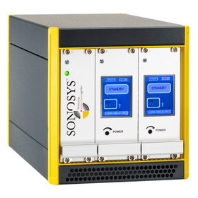

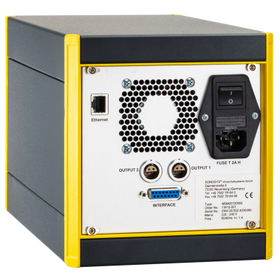
The Digital Generator is a digital control generator compatible with megasonic cleaning systems for semiconductors, electronic components, and precision instruments.
- Photomask
- Other semiconductor manufacturing equipment
- Wafer

Announcement of the product page launch for the SONOSYS Megasonic Cleaning Nozzle System | Precision Cleaning for Semiconductors and MEMS
We are pleased to announce that Tick Corporation has launched a product introduction page for the SONOSYS megasonic cleaning nozzle system. The megasonic cleaning technology from SONOSYS utilizes high-frequency energy ranging from 600 kHz to 9 MHz to precisely remove fine particles while minimizing damage to microstructures such as semiconductor wafers, photomasks, and MEMS. The new page features the characteristics of single, double, and triple nozzles, as well as applications for semiconductors, MEMS, optical components, and LCD/FPD substrates. If you are considering fine particle removal, precision cleaning using ultra-pure water (DI Water), or megasonic cleaning at frequencies such as 600 kHz or 1 MHz, please take a look.


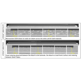
Hybrid sintering die attach adhesive as a replacement for lead solder and epoxy adhesive.
- Dedicated IC
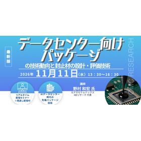

Explaining semiconductor encapsulation materials in the AI era. Learning about the latest trends in low dielectric, high thermal conductivity, and optoelectronic integration technologies.
- Other semiconductors
- plastic
- Technical Seminar
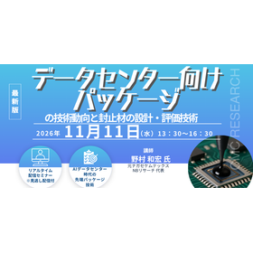
11/11 Webinar on Sealing Material Technology for Data Centers
■Title: "Technological Trends in Packaging for Data Centers and Design/Evaluation Techniques for Encapsulation Materials" This presentation will explain the packaging technologies and encapsulation materials that support semiconductor devices for data centers, which continue to evolve with the proliferation of AI. We will organize the trends of the latest packaging technologies, such as chiplets and wafer-level packaging, while systematically learning the design requirements and evaluation techniques for encapsulation materials, including high purity, moisture resistance, low stress, low dielectric loss, and high thermal conductivity. Additionally, we will introduce the latest trends in optoelectronic integration technologies that support next-generation data centers. - Technical trends in packaging for data centers - Design techniques for semiconductor encapsulation materials - Evaluation techniques for semiconductor encapsulation materials - Wafer-level packaging and chiplet technology - Latest trends in optoelectronic integration technology - Designers of semiconductor encapsulation materials - Engineers using semiconductor encapsulation materials - Developers of epoxy resins and hardeners - R&D personnel from semiconductor material manufacturers
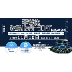
An overview of advanced packaging technologies from 2.5D/3D chiplets to thermal management, reliability evaluation, and PFAS compliance.
- Other semiconductor manufacturing equipment
- Other semiconductors
- Technical Seminar
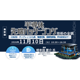
11/10 Webinar Advanced Semiconductor Packaging Technology
■Title: "The Complete Picture of Advanced Semiconductor Packaging Technology - From 2.5D/3D and Chiplets to Thermal and Power Solutions, Reliability Evaluation, and PFAS Compliance -" ――A systematic explanation of advanced packaging technologies that support the evolution of AI semiconductors. In addition to the latest technological trends in 2.5D/3D packaging, chiplets, CoWoS, TSV, and glass core substrates, you will learn broadly about manufacturing processes, yield improvement, failure analysis, reliability evaluation, PFAS regulatory compliance, and thermal and power design. Practical case studies and evaluation analysis techniques directly related to work will also be explained in detail. - Basics of semiconductor packaging technology and the evolution of trends - Latest trends in 2.5D/3D and chiplet technology - Reliability testing and failure analysis techniques - Key points for yield improvement - PFAS regulatory compliance and sustainable materials - Thermal and power design technologies for advanced packaging aimed at AI - Engineers and researchers from chemical, electronics, electrical, and automotive manufacturers - Personnel involved in semiconductor backend processes and assembly technologies - Personnel involved in materials and equipment development - Those who want to systematically learn about advanced packaging technologies
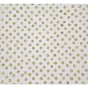

Easy diamond applications. You can trust us with peace of mind.
- Other semiconductors
- Wafer processing/polishing equipment

We provide comprehensive support from semiconductor design to embedded software development!
- Other semiconductors
- Other services
- Embedded system design service
AssetCore Technology Inc. Company Profile
Asset Core Technology Co., Ltd. provides comprehensive support from semiconductor design to embedded software development. Our "semiconductor design services" feature reliable achievements and expertise in LSI design and verification technology. In "system design development," we offer a one-stop service through collaborative design of hardware and software. Additionally, we conduct "model-based development," where engineers well-versed in MBD assist our clients' operations, as well as "embedded software development," which is grounded in an understanding of hardware.
![[Information] Basic Knowledge of No...](https://image.mono.ipros.com/public/product/image/320234/IPROS1218849934932791328.png?w=280&h=280)

Overcoming thermal displacement has been a bottleneck for achieving high precision. This is an excellent casting material developed to eliminate those bottlenecks!
- Other optical parts
- Other machine tools
- Other semiconductors


We also accommodate welding to flanges! Can be used as current introduction terminals for vacuum containers in your preferred size. We also accept small quantities, custom products, and specification ...
- Other semiconductors
- Other electronic parts
Notice of participation in the "VACUUM 2025 Vacuum Exhibition" from December 3 (Wednesday) to December 5 (Friday), 2025.
Fujidenka Co., Ltd. will be exhibiting at the "VACUUM2025 Vacuum Exhibition" held at Tokyo Big Sight. This exhibition marks the 47th edition of the comprehensive exhibition for vacuum equipment and devices. Every year, many companies and researchers involved in vacuum technology, including those in technology development, product manufacturing, and sales, attend, leading to numerous business negotiations directly related to business. We sincerely look forward to your visit.

Compatible Logic IC solutions for industrial equipment supporting 74HC, 74HCT, and 74LVC!
- Other semiconductors

Introduction to MKP Company! We possess unique patent technology that facilitates the smooth mass production of MFC.
- Other semiconductors
- controller
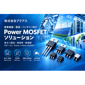
For industrial equipment, power supplies, and batteries. Supporting the selection and replacement of low on-resistance, high-efficiency, and high-reliability MOSFETs.
- Other semiconductors

This is a special industrial OPP film with a formulation of additives that is controlled as much as possible. It can be used as a release film in the electronics and optics fields without coating a re...
- Other optical parts
- Other semiconductors

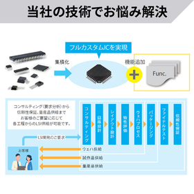
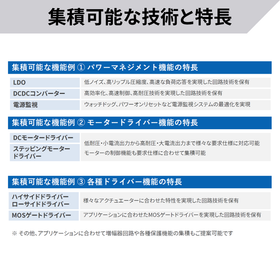
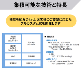
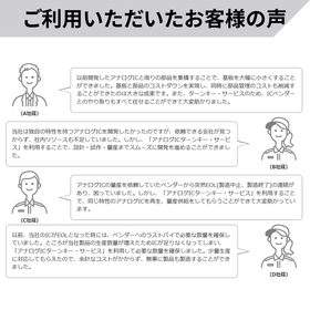
Support from the integration of discrete circuits to the regeneration of EOL products.
- Circuit board design and manufacturing
- Prototype Services
- Dedicated IC
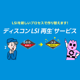
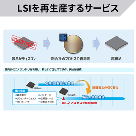
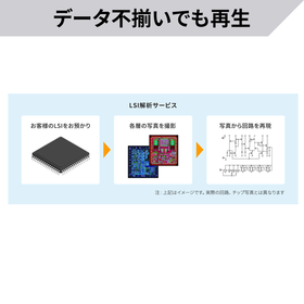
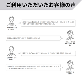
Reproduction is possible even without design data. 'Discontinued LSI Reproduction Service' that does not stop mass production and maintenance.
- Other semiconductors
- EMS
- Dedicated IC
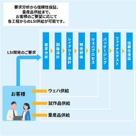
A one-stop LSI turnkey service that supports everything from organizing requirements specifications to LSI design, evaluation, prototyping, and mass production.
- Circuit board design and manufacturing
- Prototype Services
- Dedicated IC
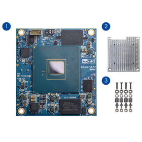

Agilex 5 FPGA SOM Second Edition. Low-cost and small Comet A13 SoM.
- Embedded Board Computers
- Other electronic parts
- Other semiconductors
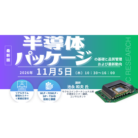
Systematically acquire semiconductor packaging technology from the basics. Learn about quality control and the latest packaging trends in one day.
- Technical Seminar
- Other semiconductor manufacturing equipment
- Other semiconductors
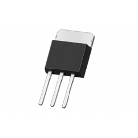

Ideal for high-side switches of 48V batteries!
- Transistor