List of Semiconductors and ICs products

  • classification:Semiconductors and ICs

811~855 item / All 4855 items

Displayed results

Reduce the workload from handling heavy objects! Here are five case studies that solved customer challenges! We are also accepting free consultations and tests tailored to your work!

  • PRエリア.png
  • Other conveying machines

Added to bookmarks

Bookmarks list

Bookmark has been removed

Bookmarks list

You can't add any more bookmarks

By registering as a member, you can increase the number of bookmarks you can save and organize them with labels.

Free membership registration

No more need to lift heavy one-gallon cans! Enjoy comfortable liquid transfer in the central kitchen.

  • Other Pumps

Added to bookmarks

Bookmarks list

Bookmark has been removed

Bookmarks list

You can't add any more bookmarks

By registering as a member, you can increase the number of bookmarks you can save and organize them with labels.

Free membership registration
画像1.jpg

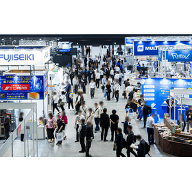
Decision to exhibit at the 1st Chubu Food Industry Creation Exhibition '26!

We will be exhibiting at the "1st Chubu Food Industry Creation Exhibition '26" to be held at Port Messe Nagoya from November 4 (Wednesday) to November 6 (Friday), 2026. As a new addition to our lineup, we will showcase the "Cordless Sanitary Handy Pump," which is a product we started selling in April last year, alongside our "Compact Sanitary Handy Pump Model MHS." - Cordless! Portable anywhere! Easy to use! Simple cleaning! It is compatible with standard 18L cans and BIB (Bag-in-Box) and features a structure that allows for easy disassembly and cleaning. We would like to invite you to visit us at this opportunity. - Venue: Port Messe Nagoya - Our exhibition booth: Hall 1 "C-66"

Added to bookmarks

Bookmarks list

Bookmark has been removed

Bookmarks list

You can't add any more bookmarks

By registering as a member, you can increase the number of bookmarks you can save and organize them with labels.

Free membership registration

Added to bookmarks

Bookmarks list

Bookmark has been removed

Bookmarks list

You can't add any more bookmarks

By registering as a member, you can increase the number of bookmarks you can save and organize them with labels.

Free membership registration

You can investigate the changes in degassing intensity while maintaining the temperature.

  • Contract Analysis
  • Memory

Added to bookmarks

Bookmarks list

Bookmark has been removed

Bookmarks list

You can't add any more bookmarks

By registering as a member, you can increase the number of bookmarks you can save and organize them with labels.

Free membership registration

The diffusion layer structure of SiC devices can be visualized (high-sensitivity evaluation of the diffusion layer structure).

  • Contract Analysis
  • Transistor

Added to bookmarks

Bookmarks list

Bookmark has been removed

Bookmarks list

You can't add any more bookmarks

By registering as a member, you can increase the number of bookmarks you can save and organize them with labels.

Free membership registration

The evaluation of the crystal structure can be performed based on the STEM images and the results of atomic composition measurements.

  • Contract Analysis
  • magnet
  • Memory

Added to bookmarks

Bookmarks list

Bookmark has been removed

Bookmarks list

You can't add any more bookmarks

By registering as a member, you can increase the number of bookmarks you can save and organize them with labels.

Free membership registration

Microscopic structural analysis of amorphous films is possible through simulation.

  • Contract Analysis
  • Memory

Added to bookmarks

Bookmarks list

Bookmark has been removed

Bookmarks list

You can't add any more bookmarks

By registering as a member, you can increase the number of bookmarks you can save and organize them with labels.

Free membership registration

It is possible to confirm the stress distribution in the sample cross-section.

  • Contract Analysis
  • Wafer

Added to bookmarks

Bookmarks list

Bookmark has been removed

Bookmarks list

You can't add any more bookmarks

By registering as a member, you can increase the number of bookmarks you can save and organize them with labels.

Free membership registration

It is possible to evaluate trace metals in ppm orders.

  • Contract Analysis
  • Ceramics
  • Wafer

Added to bookmarks

Bookmarks list

Bookmark has been removed

Bookmarks list

You can't add any more bookmarks

By registering as a member, you can increase the number of bookmarks you can save and organize them with labels.

Free membership registration

Evaluation of functional groups in graphene is possible using thermal decomposition GC/MS method.

  • Contract Analysis
  • Transistor
  • Power storage device

Added to bookmarks

Bookmarks list

Bookmark has been removed

Bookmarks list

You can't add any more bookmarks

By registering as a member, you can increase the number of bookmarks you can save and organize them with labels.

Free membership registration

Non-destructive three-dimensional observation of the internal structure of a discrete package.

  • サンプル内部構造.png
  • サンプル全景.png
  • サンプル外観.png
  • X線透過像.png
  • 開封後のサンプル内部構造.png
  • Contract Analysis
  • Other semiconductors

Added to bookmarks

Bookmarks list

Bookmark has been removed

Bookmarks list

You can't add any more bookmarks

By registering as a member, you can increase the number of bookmarks you can save and organize them with labels.

Free membership registration

Quantitative evaluation of the roughness of trench sidewalls related to device characteristics.

  • Contract Analysis
  • Other semiconductors

Added to bookmarks

Bookmarks list

Bookmark has been removed

Bookmarks list

You can't add any more bookmarks

By registering as a member, you can increase the number of bookmarks you can save and organize them with labels.

Free membership registration

Evaluation of microscopic atomic structures is possible through computational simulation.

  • Contract Analysis
  • Other semiconductors

Added to bookmarks

Bookmarks list

Bookmark has been removed

Bookmarks list

You can't add any more bookmarks

By registering as a member, you can increase the number of bookmarks you can save and organize them with labels.

Free membership registration

Reverse engineering of DRAM on the product's internal substrate.

  • Contract Analysis
  • Memory

Added to bookmarks

Bookmarks list

Bookmark has been removed

Bookmarks list

You can't add any more bookmarks

By registering as a member, you can increase the number of bookmarks you can save and organize them with labels.

Free membership registration

It is possible to obtain insights into the size and distribution of crystal grains in metallic polycrystals.

  • Contract Analysis
  • Memory

Added to bookmarks

Bookmarks list

Bookmark has been removed

Bookmarks list

You can't add any more bookmarks

By registering as a member, you can increase the number of bookmarks you can save and organize them with labels.

Free membership registration

It is possible to capture molecular information of inorganic substances in the depth direction using TOF-SIMS.

  • img_C0264_2.jpg
  • img_C0264_3_HO-Si-O.jpg
  • img_C0264_4_O-Si-O-Si-O.jpg
  • img_C0264_5_Si-N-Si.jpg
  • img_C0264_6_Si-Si.jpg
  • Contract measurement
  • Transistor
  • Memory

Added to bookmarks

Bookmarks list

Bookmark has been removed

Bookmarks list

You can't add any more bookmarks

By registering as a member, you can increase the number of bookmarks you can save and organize them with labels.

Free membership registration

Simultaneous measurement of inorganic and organic components in minute specific areas.

  • img_C0034_4.jpg
  • img_C0034_5.jpg
  • img_C0034_6.jpg
  • Contract measurement
  • Wafer
  • Memory

Added to bookmarks

Bookmarks list

Bookmark has been removed

Bookmarks list

You can't add any more bookmarks

By registering as a member, you can increase the number of bookmarks you can save and organize them with labels.

Free membership registration

We evaluate abnormalities inside the device non-destructively.

  • Contract Analysis
  • Other electronic parts
  • Transistor

Added to bookmarks

Bookmarks list

Bookmark has been removed

Bookmarks list

You can't add any more bookmarks

By registering as a member, you can increase the number of bookmarks you can save and organize them with labels.

Free membership registration

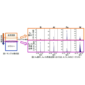
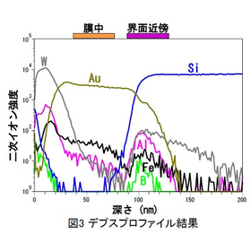
Impurities in films and interfaces such as plating can be evaluated using TOF-SIMS.
  • img_c0638_2.jpg
  • Wafer
  • Contract measurement
  • Other semiconductors

Added to bookmarks

Bookmarks list

Bookmark has been removed

Bookmarks list

You can't add any more bookmarks

By registering as a member, you can increase the number of bookmarks you can save and organize them with labels.

Free membership registration

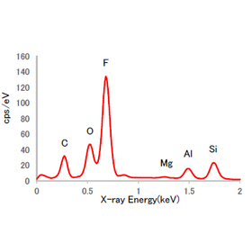
Shape observation and simple quantitative analysis using SEM-EDX.
  • img_C0736_2.jpg
  • Contract Inspection
  • Wafer
  • Other semiconductor manufacturing equipment

Added to bookmarks

Bookmarks list

Bookmark has been removed

Bookmarks list

You can't add any more bookmarks

By registering as a member, you can increase the number of bookmarks you can save and organize them with labels.

Free membership registration

It is effective to differentiate between the two methods depending on the surface structure of interest.

  • Contract Analysis
  • Memory

Added to bookmarks

Bookmarks list

Bookmark has been removed

Bookmarks list

You can't add any more bookmarks

By registering as a member, you can increase the number of bookmarks you can save and organize them with labels.

Free membership registration

High-sensitivity analysis of various solutions, such as pure water and wafer cleaning liquids, is possible.

  • Contract Analysis
  • Wafer
  • Water quality testing

Added to bookmarks

Bookmarks list

Bookmark has been removed

Bookmarks list

You can't add any more bookmarks

By registering as a member, you can increase the number of bookmarks you can save and organize them with labels.

Free membership registration

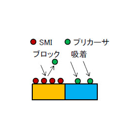
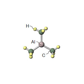
It is possible to evaluate the competitive adsorption of multiple molecules using the focus parameters for film formation (temperature, pressure).
  • img_C0743_3.jpg
  • Contract Analysis
  • Other electronic parts
  • Memory

Added to bookmarks

Bookmarks list

Bookmark has been removed

Bookmarks list

You can't add any more bookmarks

By registering as a member, you can increase the number of bookmarks you can save and organize them with labels.

Free membership registration

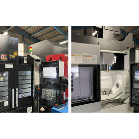
From semiconductor and LCD manufacturing equipment parts to nursing and welfare equipment parts. MINWA delivers high-precision and high-quality machining.

  • Other semiconductors
  • LCD display
  • Other machine elements

Added to bookmarks

Bookmarks list

Bookmark has been removed

Bookmarks list

You can't add any more bookmarks

By registering as a member, you can increase the number of bookmarks you can save and organize them with labels.

Free membership registration

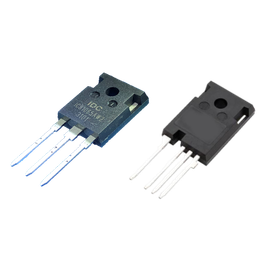
The introduction of the laminated substrate reduces the degradation of the forward characteristics of the body diode!

  • diode

Added to bookmarks

Bookmarks list

Bookmark has been removed

Bookmarks list

You can't add any more bookmarks

By registering as a member, you can increase the number of bookmarks you can save and organize them with labels.

Free membership registration

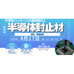
The encapsulating materials for advanced semiconductor packages require various characteristics such as low stress, moisture resistance, and high reliability. Guidelines for the design and evaluation ...

  • Other semiconductors
  • Engineering Plastics
  • Technical Seminar

Added to bookmarks

Bookmarks list

Bookmark has been removed

Bookmarks list

You can't add any more bookmarks

By registering as a member, you can increase the number of bookmarks you can save and organize them with labels.

Free membership registration

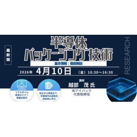
A systematic explanation from the basics of semiconductor packaging to the design and evaluation of encapsulation materials. Leading experts thoroughly organize practical perspectives from WLP/PLP to ...

  • Other semiconductor manufacturing equipment
  • Other semiconductors
  • Technical Seminar

Added to bookmarks

Bookmarks list

Bookmark has been removed

Bookmarks list

You can't add any more bookmarks

By registering as a member, you can increase the number of bookmarks you can save and organize them with labels.

Free membership registration

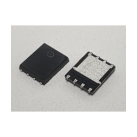
Achieve high current while minimizing losses during implementation with Power PKG (HSOP8)!

  • Transistor

Added to bookmarks

Bookmarks list

Bookmark has been removed

Bookmarks list

You can't add any more bookmarks

By registering as a member, you can increase the number of bookmarks you can save and organize them with labels.

Free membership registration

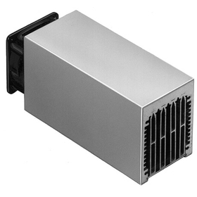
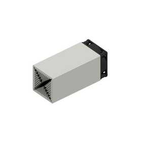
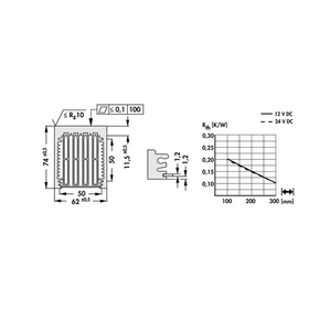
For thermal management of medium-sized devices. You can specify the ideal length in 1mm increments, without being constrained by the fixed sizes in the catalog, to match the enclosure space.
  • la6.eps.jpg
  • csm_1zeilMag_weiss_E_b78887b03c.jpg
  • Other semiconductors

Added to bookmarks

Bookmarks list

Bookmark has been removed

Bookmarks list

You can't add any more bookmarks

By registering as a member, you can increase the number of bookmarks you can save and organize them with labels.

Free membership registration

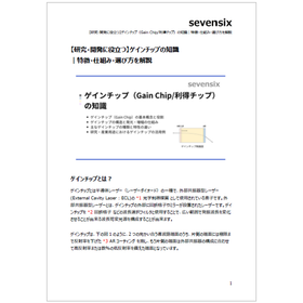
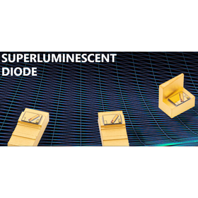
Knowledge of gain chips useful for research and development. Explanation of features, mechanisms, and how to choose.

  • diode

Added to bookmarks

Bookmarks list

Bookmark has been removed

Bookmarks list

You can't add any more bookmarks

By registering as a member, you can increase the number of bookmarks you can save and organize them with labels.

Free membership registration

Not constrained by fixed catalog sizes. You can specify the ideal length in millimeters to match thermal design and enclosure space. Additional processing can also be handled in bulk!
  • csm_1zeilMag_weiss_E_b78887b03c.jpg
  • Other semiconductors

Added to bookmarks

Bookmarks list

Bookmark has been removed

Bookmarks list

You can't add any more bookmarks

By registering as a member, you can increase the number of bookmarks you can save and organize them with labels.

Free membership registration

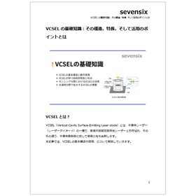
I will explain the structure, features, and key points of the application of VCSELs.

  • diode

Added to bookmarks

Bookmarks list

Bookmark has been removed

Bookmarks list

You can't add any more bookmarks

By registering as a member, you can increase the number of bookmarks you can save and organize them with labels.

Free membership registration

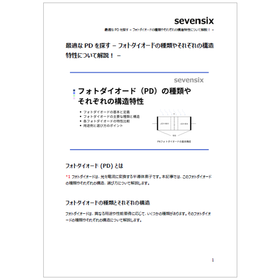
Looking for the appropriate PD. An explanation of the types of photodiodes and their structural characteristics!

  • diode

Added to bookmarks

Bookmarks list

Bookmark has been removed

Bookmarks list

You can't add any more bookmarks

By registering as a member, you can increase the number of bookmarks you can save and organize them with labels.

Free membership registration

Pin fin heat sink, width 40mm, height 20mm, length 40mm, material: Al99.5.

  • ick_s40x40x20.eps.jpg
  • csm_1zeilMag_weiss_E_b78887b03c.jpg
  • Other semiconductors

Added to bookmarks

Bookmarks list

Bookmark has been removed

Bookmarks list

You can't add any more bookmarks

By registering as a member, you can increase the number of bookmarks you can save and organize them with labels.

Free membership registration

Square pin fin heat sink, width 50mm, height 25mm, length 50mm, material: Al99.5.

  • ick_s50x50x25.eps.jpg
  • csm_1zeilMag_weiss_E_b78887b03c.jpg
  • Other semiconductors

Added to bookmarks

Bookmarks list

Bookmark has been removed

Bookmarks list

You can't add any more bookmarks

By registering as a member, you can increase the number of bookmarks you can save and organize them with labels.

Free membership registration

Achieve automation of IC packaging with space-saving design! Inspection equipment capable of high-precision 2D and 3D dimensional measurement.

  • LI700E 検査部.png
  • パッケージ画像.png
  • 検査例.png
  • 装置図?.png
  • 装置図?.png
  • 装置図?.png
  • Microcomputer

Added to bookmarks

Bookmarks list

Bookmark has been removed

Bookmarks list

You can't add any more bookmarks

By registering as a member, you can increase the number of bookmarks you can save and organize them with labels.

Free membership registration

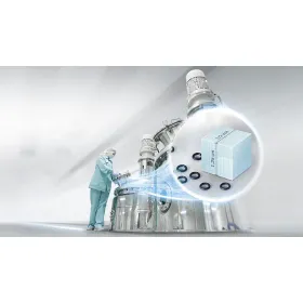
Custom formulations for important applications

  • Other semiconductors
  • Other medical supplies and cosmetic manufacturing materials
Added to bookmarks

Bookmarks list

Bookmark has been removed

Bookmarks list

You can't add any more bookmarks

By registering as a member, you can increase the number of bookmarks you can save and organize them with labels.

Free membership registration

Added to bookmarks

Bookmarks list

Bookmark has been removed

Bookmarks list

You can't add any more bookmarks

By registering as a member, you can increase the number of bookmarks you can save and organize them with labels.

Free membership registration

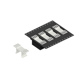
For heat dissipation of surface mount packages such as DPAK, D2PAK, and SO-8. Our compact design reliably solves thermal issues in power converters and power supply boards.
  • 1745191615.jpg
  • csm_1zeilMag_weiss_E_b78887b03c.jpg
  • Other semiconductors

Added to bookmarks

Bookmarks list

Bookmark has been removed

Bookmarks list

You can't add any more bookmarks

By registering as a member, you can increase the number of bookmarks you can save and organize them with labels.

Free membership registration

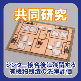
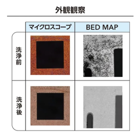
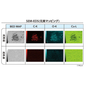
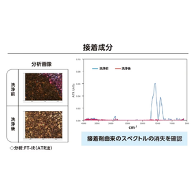
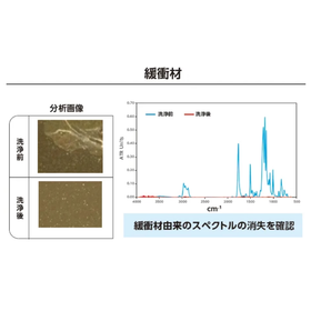
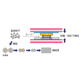
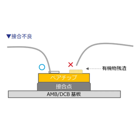
We conducted a cleaning evaluation using samples created under conditions that are likely to leave residues intentionally!
  • シンター接合後に2.png
  • シンター接合後に3.png
  • シンター接合後に4.png
  • シンター接合後に5.png
  • シンター接合後に6.png
  • シンター接合後に7.png
  • シンター接合後に8.png
  • Other semiconductors

Added to bookmarks

Bookmarks list

Bookmark has been removed

Bookmarks list

You can't add any more bookmarks

By registering as a member, you can increase the number of bookmarks you can save and organize them with labels.

Free membership registration
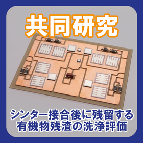
シンター接合後に残留する有機物残渣の洗浄評価.png

A page on "Cleaning evaluation of organic residue remaining after sintering" has been added.

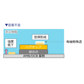
In the field of power semiconductors for automotive and industrial applications, the adoption of "sintering bonding" as a joining technology that achieves high resistance and high reliability against thermal stress is expanding, replacing solder bonding. Similar to no-clean solder bonding technology, sintering bonding is fundamentally designed to be "no-clean." However, the currently mainstream sintering bonding methods are conducted under high temperature and high pressure conditions, which can lead to the generation and adhesion of residues during the bonding process, potentially affecting subsequent processes and long-term reliability. Cleaning is one proposed solution to this issue. Although there is a "no-pressure" method for sintering bonding, its applications tend to be limited from the perspective of strength and reproducibility. Additionally, while it is residue-free, it is not "zero residue," so cleaning can also be a viable solution for achieving reliability. Detailed content of the technical column can be viewed through the related link.
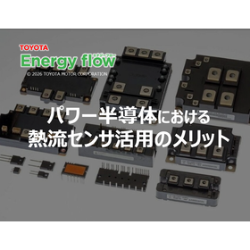
From margin design that protects by looking at temperature to confident design that attacks by looking at heat flow.

  • Dedicated IC

Added to bookmarks

Bookmarks list

Bookmark has been removed

Bookmarks list

You can't add any more bookmarks

By registering as a member, you can increase the number of bookmarks you can save and organize them with labels.

Free membership registration

Designed for a wavelength range of 760 to 2900 nm with an accuracy of ±10 nm.

  • Other semiconductors

Added to bookmarks

Bookmarks list

Bookmark has been removed

Bookmarks list

You can't add any more bookmarks

By registering as a member, you can increase the number of bookmarks you can save and organize them with labels.

Free membership registration

QCL optimal for high-precision gas detection using TDLAS.

  • Other semiconductors

Added to bookmarks

Bookmarks list

Bookmark has been removed

Bookmarks list

You can't add any more bookmarks

By registering as a member, you can increase the number of bookmarks you can save and organize them with labels.

Free membership registration

FP laser with a wavelength of 760 to 6500 nm

  • Other semiconductors

Added to bookmarks

Bookmarks list

Bookmark has been removed

Bookmarks list

You can't add any more bookmarks

By registering as a member, you can increase the number of bookmarks you can save and organize them with labels.

Free membership registration

Filter

classification
Delivery Time
Location