
List of Semiconductor inspection/test equipment products
- classification:Semiconductor inspection/test equipment
541~585 item / All 730 items


Reduce the workload from handling heavy objects! Here are five case studies that solved customer challenges! We are also accepting free consultations and tests tailored to your work!

- Other conveying machines


Strong cold wind from room temperature to -13°C! Depending on the usage environment, you can choose between the combo type or the separate type!
- Cooling system

April 10, 2024 (Wednesday) to April 12, 2024 (Friday) Notice of Participation in Nagoya Manufacturing World 2024
Sanwa Shiki Ventilator Co., Ltd. will be exhibiting at the 2024 Monozukuri World (Nagoya) held at Port Messe Nagoya. We will also be showcasing our large cooling fans and cool/warm ambient products. Date: April 10, 2024 - April 12, 2024 Opening: 10:00 AM Location: Nagoya Port Messe (Exhibition Hall 1) *Our booth: 19-1 We would be grateful if you could visit us if you have the time.


It is a device for inverting and transferring silicon wafers.
- Semiconductor inspection/test equipment
- Other semiconductor manufacturing equipment

Classified by resistivity and thickness categories.
- Semiconductor inspection/test equipment
- Other semiconductor manufacturing equipment

This is a device that detects the wafer edge using laser light and measures the diameter by comparing it with a calibration wafer (reference wafer).
- Semiconductor inspection/test equipment
- Other semiconductor manufacturing equipment

This is a device that detects the edge of a wafer and measures its diameter through image processing.
- Semiconductor inspection/test equipment
- Other semiconductor manufacturing equipment

This is a device that measures the thickness of sapphire wafers and sorts them according to their thickness.
- Semiconductor inspection/test equipment
- Other semiconductor manufacturing equipment

It is a device that measures the thickness of silicon wafers and rearranges them according to their thickness.
- Semiconductor inspection/test equipment
- Other semiconductor manufacturing equipment

It is a device that measures the thickness of silicon wafers and sorts them according to their thickness.
- Semiconductor inspection/test equipment
- Other semiconductor manufacturing equipment

It is a device that measures the thickness of silicon wafers and sorts them according to their thickness.
- Semiconductor inspection/test equipment
- Other semiconductor manufacturing equipment

This is a device used to measure the thickness of metal or resin carriers used in the silicon wafer lapping process and double-sided polishing process.
- Semiconductor inspection/test equipment
- Other semiconductor manufacturing equipment
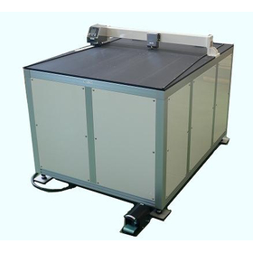
This is a device used to measure the thickness of metal or resin carriers used in the silicon wafer lapping process and the double-sided polishing process.
- Semiconductor inspection/test equipment
- Other semiconductor manufacturing equipment

This is a device used to measure the thickness of metal or resin carriers used in the silicon wafer lapping process and the double-sided polishing process.
- Semiconductor inspection/test equipment
- Other semiconductor manufacturing equipment

Thickness measurement of compound semiconductor wafers in sizes φ2”, φ4” or φ6”.
- Semiconductor inspection/test equipment
- Other semiconductor manufacturing equipment

Thickness measurement of various types of wafers below φ4"
- Semiconductor inspection/test equipment
- Other semiconductor manufacturing equipment

Thickness measurement of Si, SiC, and other wafers with a diameter of φ100mm to φ150mm.
- Semiconductor inspection/test equipment
- Other semiconductor manufacturing equipment

Thickness measurement device for silicon wafers with a diameter of φ200mm and φ300mm.
- Semiconductor inspection/test equipment
- Other semiconductor manufacturing equipment

This is a device that removes silicon wafers from a dedicated cassette and measures the thickness at the set points.
- Semiconductor inspection/test equipment
- Other semiconductor manufacturing equipment

This is a device for measuring the thickness of SiC wafers adhered to a glass plate and the thickness of the adhesive, as well as measuring the thickness of individual SiC wafers.
- Other semiconductor manufacturing equipment
- Semiconductor inspection/test equipment

The very popular TME series
- Semiconductor inspection/test equipment
- Other semiconductor manufacturing equipment

Large-diameter silicon wafer measuring instrument
- Semiconductor inspection/test equipment
- Other semiconductor manufacturing equipment

This is a device that extracts silicon wafers from a dedicated cassette using edge handling and measures the thickness of a set pattern.
- Semiconductor inspection/test equipment
- Other semiconductor manufacturing equipment

Measurement of Si wafer thickness, front and back surface P/N determination.
- Semiconductor inspection/test equipment
- Other semiconductor manufacturing equipment


We provide advanced specialized technology as an integrated R&D foundry.
- Semiconductor inspection/test equipment
- Analytical Equipment and Devices
- Other contract services


A kit has been developed to modify the current FOUP load port for N2 purge functionality within 8 hours. There have been 3,000 units delivered.

- Other semiconductor manufacturing equipment
- Semiconductor inspection/test equipment


We will provide excellent products and services at a fair price, putting ourselves in the customer's position.
- Semiconductor inspection/test equipment
- Other semiconductor manufacturing equipment


We will introduce products related to semiconductors and cleanroom equipment.
- Semiconductor inspection/test equipment
- Other semiconductor manufacturing equipment
- Other clean room equipment and facilities

Comprehensive catalog of electronic component production systems, cold forging automotive parts, and coolant-related machinery.
- Resist Device
- Etching Equipment
- Semiconductor inspection/test equipment


The semiconductor curve tracer is a state-of-the-art device capable of handling a maximum peak of 3000V and a maximum peak current of 1000A.
- Semiconductor inspection/test equipment

We will be exhibiting at Measurement Exhibition 2015 TOKYO!
We are pleased to announce that our company will be exhibiting at Measurement Expo 2015 TOKYO. We sincerely invite you to visit us. ■ Dates: December 2 (Wed) - 4 (Fri), 2015 ■ Venue: Tokyo Big Sight, Booth No. M4-34 ■ Products to be exhibited: - Semiconductor Curve Tracer CS Series - 400MHz Wideband Differential Probe BumbleBee - Japanese-made Rogowski Coil Current Probe - SE-6000 Series Isolation Probe - PSM3750 Frequency Response & Impedance Analyzer (manufactured by Newtons4th, UK) - Small Signal Amplifier - and more.

Low-cost solution for 1500A/5kV! 'Semiconductor Curve Tracer CS-5400' compatible with the latest power devices.
- Semiconductor inspection/test equipment


We propose the optimal measurement system for your development, production, and quality assurance.
- Contract manufacturing
- EMC/Static electricity measuring equipment
- Semiconductor inspection/test equipment


Transport, stack, and send the film non-contact.
- Other industrial robots
- Semiconductor inspection/test equipment
- Other machine elements

Justem Co., Ltd., manufacturer and seller of measuring machines, processing machines, dedicated machines, and automation equipment.
- Contract manufacturing
- Semiconductor inspection/test equipment
- Other semiconductor manufacturing equipment


Compatible with 6, 8, and 12 inches. There is also taping available from a dedicated tray. We also accept custom production of taping devices.
- Taping Machine
- Semiconductor inspection/test equipment


Prevents slight misalignment of devices, improving operability even when using high-magnification microscopes.
- Semiconductor inspection/test equipment
- Circuit Board Inspection Equipment
- probe


An essential tool for measuring wafer temperature distribution.
- Semiconductor inspection/test equipment
- Temperature and humidity measuring instruments


This is an MBE device compatible with compact sizes (1 inch to 2 inches).
- Vacuum Equipment
- Semiconductor inspection/test equipment
- Evaporation Equipment


500℃ temperature cycle thin film stress measurement device FLX-2320-S
- Semiconductor inspection/test equipment


Ceramic bearing
- Heat exchanger
- Semiconductor inspection/test equipment
- Food Processing Equipment


The cooperative test system will accommodate inspections of all types of circuit boards.
- Semiconductor inspection/test equipment
- Circuit Board Inspection Equipment
- Visual Inspection Equipment


A soundproof shield room that combines electromagnetic shielding performance and sound insulation performance, creating an excellent inspection environment!
- Semiconductor inspection/test equipment
- Other inspection equipment and devices
- X-ray inspection equipment

This is the 'Scanner System CS-700 Series' that automatically switches measuring devices!
- Semiconductor inspection/test equipment
- Other electronic parts
- oscilloscope

On June 4, 2013, Iwattsu Measurement began selling the "Scanner System CS-700 Series."
Iwatou Keisoku Co., Ltd. will release the "Scanner System CS-700 Series," which automatically switches measurement devices for the "Semiconductor Curve Tracer CS Series" that has been available for some time. The release will start on June 4, 2013, with orders expected to begin immediately, and the price will vary depending on specifications. Iwatou Keisoku anticipates selling 50 units of the CS-700 Series over the next year. The CS-700 Series supports automatic measurement of various devices by combining relay units, allowing for signal switching of up to 10 channels with a single relay unit. Additionally, by adding CS-701, it is possible to expand the system with up to 800 relay units. This enables the construction of an extremely flexible system. Furthermore, when combined with CS-810 (semiconductor parameter measurement software: a common option for the CS Series), it allows for large-scale automatic measurements of devices. This eliminates the wiring work that was previously necessary for each measurement, significantly improving experimental and evaluation tasks. For more details, please contact us or refer to the materials.


We handle everything from development and design to processing, welding, assembly, and inspection consistently.
- Vacuum Equipment
- Semiconductor inspection/test equipment
- Other inspection equipment and devices


High acceleration testing (up to 34,000 rpm, 100,000 G). Temperature control within the chamber is possible. Complies with standards such as JIS, MIL, and IEC.
- Other semiconductor manufacturing equipment
- Semiconductor inspection/test equipment

Detects foreign particles in devices. Capable of testing over 2000 parts per hour.
- Other semiconductor manufacturing equipment
- Semiconductor inspection/test equipment
- Testing Equipment and Devices


It is a manufacturer of IC programmers certified by major semiconductor manufacturers worldwide, produced by "Leap Corporation" in Taiwan.
- Semiconductor inspection/test equipment

It is a manufacturer of IC programmers certified by major semiconductor manufacturers around the world, produced by "Taiwan Leap Company."
- Semiconductor inspection/test equipment