We have compiled a list of manufacturers, distributors, product information, reference prices, and rankings for microscope.
ipros is IPROS GMS IPROS One of the largest technical database sites in Japan that collects information on.

microscope Product List and Ranking from 178 Manufacturers, Suppliers and Companies | IPROS GMS

Last Updated: Aggregation Period:Jan 14, 2026~Feb 10, 2026
This ranking is based on the number of page views on our site.

microscope Manufacturer, Suppliers and Company Rankings

Last Updated: Aggregation Period:Jan 14, 2026~Feb 10, 2026
This ranking is based on the number of page views on our site.

  1. null/null
  2. スリーアールソリューション Fukuoka//Trading company/Wholesale
  3. アズサイエンス 松本本社 Nagano//Trading company/Wholesale
  4. 4 アイテス Shiga//Electronic Components and Semiconductors
  5. 5 サーモフィッシャーサイエンティフィック株式会社/Thermo Fisher Scientific K.K. Tokyo//Testing, Analysis and Measurement

microscope Product ranking

Last Updated: Aggregation Period:Jan 14, 2026~Feb 10, 2026
This ranking is based on the number of page views on our site.

  1. White interference microscope equipped with laser microscope 'VK-X3000'
  2. White interference microscope equipped with laser 'VK-X4000 series'
  3. All-in-one fluorescence microscope 'BZ-X1000 Series'
  4. 4 Portable Microscope "Magic Loupe R" / 15x Magnification, Photo and Save Capability スリーアールソリューション
  5. 5 All-in-one fluorescence microscope 'BZ-X800'

microscope Product List

91~120 item / All 650 items

Displayed results

Analysis of electronic components and materials using TEM.

TEM (Transmission Electron Microscope) meets a wide range of requirements for observing failure sites of electronic components, length measurements, elemental analysis, crystal structure analysis, and material evaluation.

TEM can perform not only high-magnification observation but also elemental analysis using EDS and EELS, as well as analysis of crystal structure, surface orientation, lattice constants, and more through electron diffraction.

  • Contract Analysis
  • Other semiconductors
  • Other contract services
  • microscope

Added to bookmarks

Bookmarks list

Bookmark has been removed

Bookmarks list

You can't add any more bookmarks

By registering as a member, you can increase the number of bookmarks you can save and organize them with labels.

Free membership registration

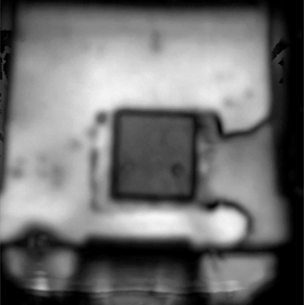
Crystal analysis by EBSD BGA

The EBSD method allows for the estimation of crystal states and residual stresses! Here is an example of BGA analysis.

Here is an example of the analysis of BGA (Ball Grid Array). In the observation using a microscope, both optical microscopy and SEM are employed. In the crystal analysis using the EBSD method, we utilize the Phase map, Sn Grain map, Sn IPF map, and Sn GROD map, which allow for the inference of crystal states and residual stresses. 【Overview】 ■ Crystal analysis using the EBSD method - Phase map - Sn Grain map - Sn IPF map - Sn GROD map *For more details, please refer to the PDF materials or feel free to contact us.

  • image_02.png
  • image_03.png
  • image_04.png
  • image_05.png
  • image_06.png
  • Analytical Equipment and Devices
  • Analysis Services
  • microscope

Added to bookmarks

Bookmarks list

Bookmark has been removed

Bookmarks list

You can't add any more bookmarks

By registering as a member, you can increase the number of bookmarks you can save and organize them with labels.

Free membership registration

[Contract Analysis] Laser Microscope (High-Precision 3D Measurement & Color Observation)

It is possible to perform 3D measurements of the surface roughness of samples and surface shape measurements through transparent objects!

We offer contract analysis using the shape measurement laser microscope "VK-X200." Observations and measurements are conducted using a 408nm laser. The measurement results are based on a traceability system that connects to national standards, allowing the measurement equipment to be used for non-destructive testing. The laser microscope enables 3D measurement of the surface roughness of samples, as well as measurement of the thickness of transparent films and surface shapes through transparent materials. 【Features】 ■ Capable of 3D measurement of surface roughness of samples ■ Capable of measuring the thickness of transparent films and surface shapes through transparent materials ■ Observations and measurements are conducted using a 408nm laser ■ Measurement results are based on a traceability system that connects to national standards ■ Can be utilized as non-destructive testing equipment *For more details, please refer to the PDF document or feel free to contact us.

  • 2020-08-05_10h07_07.png
  • 2020-08-05_10h07_31.png
  • 2020-08-05_10h07_44.png
  • 2020-08-05_10h07_57.png
  • Contract Inspection
  • Contract Analysis
  • Contract measurement
  • microscope

Added to bookmarks

Bookmarks list

Bookmark has been removed

Bookmarks list

You can't add any more bookmarks

By registering as a member, you can increase the number of bookmarks you can save and organize them with labels.

Free membership registration

Observation of the diffusion layer of SiC MOSFET using LV-SEM and EBIC methods.

Even with SiC power devices, we can provide consistent support for cross-section preparation of specific areas, observation of diffusion layer shapes, as well as wiring structure and crystal structure analysis!

Our company conducts observations of the diffusion layer of SiC MOSFETs using LV-SEM and EBIC methods. We can perform cross-section fabrication of specific areas using FIB, shape observation of the diffusion layer using LV-SEM/EBIC, and further through analyses of wiring structures and crystal structures using TEM, all applicable to SiC power devices. In "LV-SEM diffusion layer observation," secondary electrons (SE2) influenced by the built-in potential of the PN junction are detected with the Inlens detector. The shape of the diffusion layer can be visualized through SEM observation of the FIB cross-section. [Analysis methods using EBIC] ■ PEM/OBIRCH defect location identification ■ FIB cross-section processing ■ Low acceleration SEM ■ EBIC analysis ■ TEM *For more details, please refer to the PDF document or feel free to contact us.

  • 2020-08-18_15h03_09.png
  • 2020-08-18_15h03_13.png
  • 2020-08-18_15h03_19.png
  • 2020-08-18_15h03_24.png
  • Analysis Services
  • Contract Analysis
  • microscope

Added to bookmarks

Bookmarks list

Bookmark has been removed

Bookmarks list

You can't add any more bookmarks

By registering as a member, you can increase the number of bookmarks you can save and organize them with labels.

Free membership registration

Crack observation using a tabletop SEM (scanning electron microscope).

Fine cracks are easy to see! No conductive treatment is required, allowing for quick and detailed observation.

Introducing "Crack Observation Using Tabletop SEM (Scanning Electron Microscope)." In the evaluation of product reliability, cross-sectional observation of cracks is essential. While optical microscopy may overlook small cracks, SEM observation allows for clear identification. Moreover, with a tabletop SEM, no conductive treatment is necessary, enabling quick and detailed observation. 【Features】 ■ No need for deposition ■ Easy visibility of crystal grains ■ Fine cracks are easily visible *For more details, please refer to the PDF document or feel free to contact us.

  • image_18.png
  • image_20.png
  • Electron microscope
  • Contract Analysis
  • Contract Inspection
  • microscope

Added to bookmarks

Bookmarks list

Bookmark has been removed

Bookmarks list

You can't add any more bookmarks

By registering as a member, you can increase the number of bookmarks you can save and organize them with labels.

Free membership registration

[Data] Cross-sectional observation of neodymium magnets using a tabletop SEM (scanning electron microscope)

We have published cross-sectional observations in clear vision mode and normal/standard mode!

This document introduces the cross-sectional observation of neodymium magnets using a tabletop SEM (scanning electron microscope). Samples with magnetic properties, such as neodymium magnets, cannot be observed in a magnetized state using SEM; however, by applying demagnetization treatment, SEM observation and elemental analysis can be performed. Please take a moment to read it. 【Contents】 ■ Demagnetization of neodymium magnets and cross-sectional observation using SEM (Hitachi High-Tech TM3030Plus) - Demagnetization treatment (SEM observation of the magnet in a magnetized state is not possible, so demagnetization is performed) - Cross-sectional observation - Elemental analysis using EDX *For more details, please refer to the PDF document or feel free to contact us.

  • Electron microscope
  • Contract Analysis
  • Contract Inspection
  • microscope

Added to bookmarks

Bookmarks list

Bookmark has been removed

Bookmarks list

You can't add any more bookmarks

By registering as a member, you can increase the number of bookmarks you can save and organize them with labels.

Free membership registration

Cross-sectional observation of large samples (expansion valve)

Introducing a case study on the cross-section preparation of a large sample (65mm × 28mm) and the observation of its internal structure!

We present an observation case of a large sample (expansion valve) measuring 65mm × 28mm. This sample uses magnetic materials, and due to distortion in the images during SEM observation, we primarily conducted observations using an optical microscope. From the appearance and X-ray radiographic observation, it was found that there are some areas that are not visible in the X-ray. [Overview] ■ Appearance and X-ray radiographic observation ■ Cross-sectional observation using an optical microscope *For more details, please refer to the PDF document or feel free to contact us.

  • image_02.png
  • image_04.png
  • image_05.png
  • image_10.png
  • image_03.png
  • image_11.png
  • image_12.png
  • image_13.png
  • image_14.png
  • Other contract services
  • Contract Analysis
  • Contract Inspection
  • microscope

Added to bookmarks

Bookmarks list

Bookmark has been removed

Bookmarks list

You can't add any more bookmarks

By registering as a member, you can increase the number of bookmarks you can save and organize them with labels.

Free membership registration

Differences in appearance due to SEM observation conditions

Introducing SEM images taken under various conditions! An explanation of the differences in appearance based on SEM observation conditions.

SEM observation involves detecting secondary electrons and backscattered electrons generated when electrons irradiate the surface of the sample and scatter in the outermost layer of the sample. These are captured by a detector and displayed as an image on a monitor. There are various types of detectors for capturing electrons, each producing images that leverage their unique characteristics, and the appearance can change by varying the acceleration voltage. In this document, we introduce SEM images captured under various conditions. We encourage you to read it. [Contents] ■ Backscattered Electron Images - Backscattered electron images at high acceleration voltage (AsB detector) - Backscattered electron images at low acceleration voltage (EsB detector) ■ Secondary Electron Images - Differences in appearance based on acceleration voltage - Differences in appearance based on detector position *For more details, please refer to the PDF document or feel free to contact us.

  • SEM_3kV-15kV.png
  • Other contract services
  • microscope

Added to bookmarks

Bookmarks list

Bookmark has been removed

Bookmarks list

You can't add any more bookmarks

By registering as a member, you can increase the number of bookmarks you can save and organize them with labels.

Free membership registration

FE-SEM observation (Crystal grain observation of Al wire bonding section)

High-brightness electron gun for detailed SEM images! Equipped with an in-lens SE detector sensitive to surface information.

The ZEISS "FE-SEM ULTRA55" is equipped with a GEMINI column, allowing for high-resolution observation at extremely low acceleration voltages. It also features multiple detectors, enabling the observation of various samples. Composition information can be obtained using two types of backscattered electron detectors, and high-resolution EDX analysis can be performed even at low acceleration voltages. 【Features】 ■ High-brightness electron gun for detailed SEM images ■ Ultra-surface analysis at extremely low acceleration voltages ■ In-lens SE detector sensitive to surface information ■ Composition information obtained from two types of backscattered electron detectors ■ High-resolution EDX analysis even at low acceleration voltages ■ Observation without deposition *For more details, please refer to the PDF document or feel free to contact us.

  • 2021-07-02_14h57_55.png
  • 2021-07-02_14h58_07.png
  • 2021-07-02_14h58_14.png
  • 2021-07-02_14h58_22.png
  • 2021-07-02_14h58_32.png
  • Analytical Equipment and Devices
  • Other contract services
  • microscope

Added to bookmarks

Bookmarks list

Bookmark has been removed

Bookmarks list

You can't add any more bookmarks

By registering as a member, you can increase the number of bookmarks you can save and organize them with labels.

Free membership registration

Observation of the coating film

Introducing examples of observation and analysis of coating films used in various products, including "microtomes" capable of planar inclined cutting!

We will introduce examples of observation and analysis of coating films used in various products such as automobiles and mobile phones. The "Triple Ion Polisher (CP)" can process samples containing both hard and soft materials without causing damage, while the "Microtome" is capable of not only producing cross-sections but also performing planar inclined cutting. Additionally, the "Desktop Inclined Cutting Machine" can extract sample surfaces that are 6 to 300 times the original thickness as surface information, and the "Desktop SEM (Scanning Electron Microscope)" has a mode for observation under low vacuum (charge reduction), allowing for the observation and elemental analysis of samples that release volatile components. [Observation of Plastic Coating (Mobile Phone Case)] ■ Triple Ion Polisher (CP) ■ Microtome ■ Desktop Inclined Cutting Machine ■ Desktop SEM (Scanning Electron Microscope) *For more details, please refer to the PDF document or feel free to contact us.

  • 斜め切削機_2.png
  • 斜め切削機_3.png
  • Analytical Equipment and Devices
  • Other environmental analysis equipment
  • microscope

Added to bookmarks

Bookmarks list

Bookmark has been removed

Bookmarks list

You can't add any more bookmarks

By registering as a member, you can increase the number of bookmarks you can save and organize them with labels.

Free membership registration

Ultrasonic Microscope 'SAM'

Non-destructive observation is possible! It is effective in detecting defects in internal conditions and adhesion states!

We would like to introduce our ultrasonic microscope, the SAM (Scanning Acoustic Microscope). It is highly effective in detecting defects in the internal conditions and adhesion states of semiconductor packages, substrates, and electronic components. Observation can be performed non-destructively, and defects such as delamination can be detected from the reflected waves of the ultrasonic waves incident on the sample. 【Specifications (excerpt)】 ■ Pulse Receiver: 500MHz ■ Observation Methods: Compatible with both reflection and transmission methods ■ Acoustic Lenses / Reflection Method: 15, 25, 30, 50, 80, 100, 230MHz ■ Acoustic Lenses / Transmission Method: 15, 25, 30, 50, 100MHz *For more details, please refer to the PDF document or feel free to contact us.

  • Other microscopes
  • microscope

Added to bookmarks

Bookmarks list

Bookmark has been removed

Bookmarks list

You can't add any more bookmarks

By registering as a member, you can increase the number of bookmarks you can save and organize them with labels.

Free membership registration

Cross-sectional observation of substrate-mounted components (1) to (6)

Introducing the "Observation Mode" of a chip capacitor (MLCC) under a microscope!

We would like to introduce an example of cross-sectional observation of mounted components conducted by our company. Using commercially available computer circuit boards, we observed the solder joints of mounted components and the internal structures of the components with a metallurgical microscope. The observation modes of the metallurgical microscope include bright field observation, dark field observation, and polarized light observation, among others. Additionally, there are observations using transmitted light, and the observation mode is selected according to the sample. By conducting cross-sectional observations before and after reliability testing, we can evaluate the reliability of the product. When observing, it is important to select an appropriate "observation mode" to clearly capture the condition of the solder joint interface and defects such as cracks. [Case Overview] ■ Using commercially available computer circuit boards ■ Observing the solder joints of mounted components and the internal structures of the components with a metallurgical microscope ・Observation modes: bright field observation, dark field observation, polarized light observation, etc. *For more details, please refer to the PDF document or feel free to contact us.

  • Circuit board design and manufacturing
  • microscope

Added to bookmarks

Bookmarks list

Bookmark has been removed

Bookmarks list

You can't add any more bookmarks

By registering as a member, you can increase the number of bookmarks you can save and organize them with labels.

Free membership registration

Announcement of the introduction of Talos F200E

Improved resolution for TEM and STEM! Performance has been significantly enhanced, allowing for EDS analysis with four detectors.

Our company will introduce the FEI "Talos F200E" transmission electron microscope system. Compared to conventional models, the resolution of TEM and STEM has improved, and performance has been significantly enhanced, including the capability for EDS analysis with four detectors. Additionally, it is equipped with Drift Corrected Frame Integration (DCFI), which allows for the integration of multiple frames while correcting for drift. 【Specifications (excerpt)】 ■ Acceleration Voltage: 200kV, 80kV ■ TEM Information Limit: ≦0.11nm ■ STEM Resolution: ≦0.14nm ■ Drift Corrected Frame Integration (DCFI) ・Integration of multiple frames while correcting for drift *For more details, please download the PDF or feel free to contact us.

  • Other microscopes
  • Transmission electron microscope
  • microscope

Added to bookmarks

Bookmarks list

Bookmark has been removed

Bookmarks list

You can't add any more bookmarks

By registering as a member, you can increase the number of bookmarks you can save and organize them with labels.

Free membership registration

Ultrasonic microscope observation of semiconductor packages

Ultrasonic microscope observation of transistors! It is possible to check the peeling conditions at various locations even with the same focus.

We would like to introduce our ultrasonic microscope observation of semiconductor packages. Due to storage conditions and mounting conditions, delamination can occur between the metal parts (die pad) and the package resin in semiconductor packages. Delamination inside the package is a defect that significantly affects product quality, but it cannot be confirmed visually from the outside. By using an ultrasonic microscope, we can clearly capture the internal structure of the package and contribute to reliability evaluation. 【Features】 ■ Ultrasonic microscope observation from the chip side - By changing the focal position, previously unseen areas of the same sample become visible. ■ Ultrasonic microscope observation from the die pad side - Delamination conditions can be confirmed at various locations even with the same focus. *For more details, please download the PDF or feel free to contact us.

  • Contract Analysis
  • Analysis Services
  • Contract Analysis
  • microscope

Added to bookmarks

Bookmarks list

Bookmark has been removed

Bookmarks list

You can't add any more bookmarks

By registering as a member, you can increase the number of bookmarks you can save and organize them with labels.

Free membership registration

Wireless Digital Microscope '3R-WM601WIFI'

Achieving wireless operation! It performs well even in environments where the cord made it difficult to use the microscope.

The "3R-WM601WIFI" is a wireless digital microscope that displays images captured by the microscope on a tablet or smartphone with WiFi functionality. Captured data can also be saved directly within the device. Additionally, it supports both wireless and wired connections, allowing you to choose the connection method according to the usage environment, such as using a wired connection in environments with wireless restrictions. 【Features of the dedicated app】 ■ Can compare with dual screen display ■ Allows continuous measurement within the same image ■ Measured values can be used in other images ■ Can save correction results ■ Scale display is possible *For more details, please refer to the PDF document or feel free to contact us.

  • Other microscopes
  • microscope

Added to bookmarks

Bookmarks list

Bookmark has been removed

Bookmarks list

You can't add any more bookmarks

By registering as a member, you can increase the number of bookmarks you can save and organize them with labels.

Free membership registration

Optical microscope transmission phase-shift laser interference microscope

Optical microscope transmission phase-shifting laser interference microscope

This is a new type of microscope positioned above conventional optical microscopes, capable of measuring refractive index distribution and thickness structure quickly and quantitatively, and visualizing it in three dimensions. 【Features】 ○ By applying laser interference methods, it can non-contact measure the refractive index and height of samples. ○ High speed… measurement time is a few seconds ○ High precision… phase measurement accuracy ±(1/150) λ, refractive index difference measurement accuracy ±0.0001, height measurement accuracy ±0.2μm ○ Spatial resolution… equivalent to optical microscopes ● For more details, please contact us or download the catalog.

  • Optical microscope
  • microscope

Added to bookmarks

Bookmarks list

Bookmark has been removed

Bookmarks list

You can't add any more bookmarks

By registering as a member, you can increase the number of bookmarks you can save and organize them with labels.

Free membership registration

(S)TEM (Scanning Transmission Electron Microscopy)

Elemental analysis, state evaluation, particle size analysis, and acquisition of three-dimensional structural images at the nanoscale.

TEM (Transmission Electron Microscopy) is a method that involves irradiating a thin sample with an electron beam, imaging the electrons that have passed through or scattered from the sample, and observing it at high magnification. ■ Advantages - Enlarged images can be obtained with sub-nanometer spatial resolution, allowing for the observation and analysis of the sample's fine structure and lattice defects. - It is possible to evaluate the crystallinity of the sample and identify materials. - By fabricating samples using FIB (Focused Ion Beam), it is possible to observe specific locations within a device with pinpoint accuracy. - By combining optional features, it is also possible to analyze the composition and state of localized areas. ■ Disadvantages - It is necessary to thin the sample (in some cases, thinning may be difficult for certain samples). - It does not observe individual atoms but rather displays average information in the thickness direction of the sample (typically about 0.1 μm thick). - Sample processing and observation may lead to alteration or deformation of the sample.

  • 打ち合わせ.jpg
  • セミナー.jpg
  • Contract Analysis
  • Contract measurement
  • Contract Inspection
  • microscope

Added to bookmarks

Bookmarks list

Bookmark has been removed

Bookmarks list

You can't add any more bookmarks

By registering as a member, you can increase the number of bookmarks you can save and organize them with labels.

Free membership registration

[EMS] Emission Microscopy Method

Rapid identification of the malfunctioning area.

EMS is a method that quickly identifies the location of faults by detecting weak light emissions caused by abnormal operation of semiconductor devices. It is also referred to as EMMS, PEM, or EMI. - Only transparent materials can be evaluated in the measurement wavelength range (from the visible to near-infrared region). - It is possible to capture internal defects such as cracks, crystal defects, oxide film breakdown due to ESD, and shorts caused by Al spikes with low damage.

  • 打ち合わせ.jpg
  • セミナー.jpg
  • Contract Analysis
  • Contract measurement
  • Contract Inspection
  • microscope

Added to bookmarks

Bookmarks list

Bookmark has been removed

Bookmarks list

You can't add any more bookmarks

By registering as a member, you can increase the number of bookmarks you can save and organize them with labels.

Free membership registration

[SIM] Scanning Ion Microscopy Method

Observation of SIM images is possible with high resolution (accelerating voltage 30kV: 4nm).

- SIM imaging observation is possible with high resolution (accelerating voltage 30kV: 4nm). - Compared to SEM images, SIM images provide information about the extreme surface layer. - Observation of metal crystal grains is possible (e.g., Al, Cu). - The resolution is inferior to SEM images (SIM: 4nm, SEM: 0.5nm). ■Features of MST-owned equipment - Compatible with JEIDA standard wafers with a maximum sample size of 300mm in diameter. - Continuous cross-sectional SIM imaging acquisition is possible in combination with FIB (Focused Ion Beam) processing (Slice & View).

  • 打ち合わせ.jpg
  • セミナー.jpg
  • Contract Analysis
  • Contract measurement
  • Contract Inspection
  • microscope

Added to bookmarks

Bookmarks list

Bookmark has been removed

Bookmarks list

You can't add any more bookmarks

By registering as a member, you can increase the number of bookmarks you can save and organize them with labels.

Free membership registration

[Analysis Case] Evaluation of the Diffusion Layer Structure of Bipolar Transistors

Clearly observable structure of the diffusion layer including pn junction determination.

It is possible to observe in detail from an overview of the NPN bipolar transistors within commercially available LSI to an enlarged view of the emitter section. This is an example where a cross-section passing through the center of the emitter electrode was exposed, and AFM observation and SCM measurement were conducted. By overlaying the AFM image, the positional relationship with the wiring becomes clear.

Added to bookmarks

Bookmarks list

Bookmark has been removed

Bookmarks list

You can't add any more bookmarks

By registering as a member, you can increase the number of bookmarks you can save and organize them with labels.

Free membership registration

[Analysis Case] Evaluation of Specific Crystalline Grains in CIGS Thin-Film Solar Cells

Observation of orthogonal cross-sections at locations with characteristics identified in EBIC measurements of arbitrary cross-sections.

Insights into the relationship between electrical properties and crystals can be obtained through EBIC and EBSD, but the depth of information differs. For areas where electrical properties were characteristic in the EBIC distribution measurement, we created cross-sectional samples and conducted STEM imaging in the depth direction. Additionally, we measured electron diffraction for each crystal grain. This further clarified the relationship between electrical properties and crystal grains and grain boundaries. By performing STEM observation and electron diffraction measurements, it is possible to obtain localized information about specific crystal grains.

Added to bookmarks

Bookmarks list

Bookmark has been removed

Bookmarks list

You can't add any more bookmarks

By registering as a member, you can increase the number of bookmarks you can save and organize them with labels.

Free membership registration

[Analysis Case] Evaluation of the Mixed State of the Active Layer in Organic Thin-Film Solar Cells

Evaluation of the distribution state of organic materials using low-energy STEM observation and EELS measurement.

By using low-energy STEM observation and STEM-EELS surface analysis, we evaluated the mixed state of the active layer in bulk heterojunction solar cells. For the evaluation, samples were prepared with only the active layer deposited on ITO. The contrast in the low-energy STEM image (Photo 1) corresponds to the elemental distribution of S and C in the STEM-EELS images (Photos 2 and 3), confirming that it reflects the bulk heterostructure. Additionally, a bias in the distribution of S was observed, suggesting that P3HT is segregated towards the surface side.

Added to bookmarks

Bookmarks list

Bookmark has been removed

Bookmarks list

You can't add any more bookmarks

By registering as a member, you can increase the number of bookmarks you can save and organize them with labels.

Free membership registration

[Analysis Case] Observation of Heterojunction Interface in CIGS Thin-Film Solar Cells

Evaluation of the crystal structure of the high-resistance layer at the CdS/CIGS junction interface using ultra-high-resolution STEM.

We directly observed the CdS/CIGS heterojunction interface using a Cs-corrected STEM device. TEM images, high-resolution HAADF-STEM images, and simulations using first-principles calculations confirmed that CIGS and CdS are heteroepitaxially joined.

Added to bookmarks

Bookmarks list

Bookmark has been removed

Bookmarks list

You can't add any more bookmarks

By registering as a member, you can increase the number of bookmarks you can save and organize them with labels.

Free membership registration

[Analysis Case] Resistance Evaluation of Heterojunction Interface in CIGS Solar Cells

Evaluation of local resistance distribution using scanning spreading resistance microscopy (SSRM) under vacuum.

The heterojunction interface of ZnO/CdS/CIGS in CIGS thin-film solar cells was analyzed using the SSRM method, and the local resistance distribution was measured. By conducting measurements in a vacuum environment, we were able to remove adsorbed water from the measurement surface and achieve high spatial resolution. The measurement results indicate that we can measure the resistance values of each layer with nanometer-level spatial resolution. The resistance values of each layer differ by several orders of magnitude, indicating differences in carrier concentration. It was found that the CIGS layer has a higher resistance than the i-ZnO layer, and that CdS has an even higher resistance than these layers.

Added to bookmarks

Bookmarks list

Bookmark has been removed

Bookmarks list

You can't add any more bookmarks

By registering as a member, you can increase the number of bookmarks you can save and organize them with labels.

Free membership registration

[Analysis Case] Cross-Section Observation of Organic Thin-Film Solar Cells

Using low acceleration voltage STEM, slight density differences in organic films can be observed.

In bulk heterojunction solar cells using mixed films of p-type and n-type materials, it is necessary to appropriately control the mixing state of the materials within the film for high efficiency. In films with low density (such as organic films), it is difficult to achieve contrast using a dedicated TEM machine at high acceleration voltages (several hundred kV) due to the high transmission of the electron beam. On the other hand, in STEM imaging at low acceleration voltages, where slight differences in density are reflected, the mixing state within the film can be clearly observed.

Added to bookmarks

Bookmarks list

Bookmark has been removed

Bookmarks list

You can't add any more bookmarks

By registering as a member, you can increase the number of bookmarks you can save and organize them with labels.

Free membership registration

[Analysis Case] Observation of Crystal Structure of Multicomponent Metallic Nanoparticles by TEM

Ultra-high resolution STEM observation of InGaZnO4 particles

The STEM device equipped with a Cs collector (spherical aberration correction function) enables ultra-high-resolution observation (resolution of 0.10 nm). The HAADF*-STEM image, which is sensitive to atomic weight, is an effective tool for directly understanding multi-component crystal structures. In this study, we evaluated micro-particles in oxide semiconductors, which can be applied to the atomic arrangement at heterogeneous material interfaces and compound interfaces, as well as grain boundary segregation assessments. *High-Angle Annular Dark-Field: Contrast is obtained that is proportional to atomic weight (Z).

Added to bookmarks

Bookmarks list

Bookmark has been removed

Bookmarks list

You can't add any more bookmarks

By registering as a member, you can increase the number of bookmarks you can save and organize them with labels.

Free membership registration

[Analysis Case] Cross-sectional Observation of TEM/SEM Organic EL and Gate Oxide Film

Low-acceleration STEM observation allows for contrast even in low-density membranes.

For membranes with low density, it is difficult to achieve contrast at high acceleration voltages (hundreds of kV) due to the high transmission capability of the electron beam. However, in low acceleration voltage SEM-STEM images, slight differences in density can be reflected, allowing for clear composition contrast. This can be applied to organic EL films, low-k films, gate oxide films, TEOS films, BPSG films, etc., where the differences in density, average mass, and composition are small. 1) STEM observation using SEM equipment with lower acceleration voltage compared to dedicated TEM equipment. Measurement methods: TEM, SEM Product fields: LSI, memory, display, solar cells, lighting Analysis purposes: Shape evaluation, film thickness evaluation For more details, please download the materials or contact us.

Added to bookmarks

Bookmarks list

Bookmark has been removed

Bookmarks list

You can't add any more bookmarks

By registering as a member, you can increase the number of bookmarks you can save and organize them with labels.

Free membership registration

[Slice&View] Three-Dimensional SEM Observation Method

By repeatedly performing cross-sectioning processing with FIB and observation with SEM, and reconstructing the obtained images, three-dimensional structural information can be obtained.

Using a high-resolution SEM device equipped with FIB, we can obtain three-dimensional structural information by repeatedly performing cross-sectioning (Slice) with FIB and observing (View) with SEM, and then reconstructing the acquired images. Similarly, Slice & View is also possible for SIM (Scanning Ion Microscope) images. - It is possible to observe secondary electron (SE), backscattered electron (BSE) images, and scanning ion microscope (SIM) images.

  • 打ち合わせ.jpg
  • セミナー.jpg
  • Contract Analysis
  • Contract measurement
  • Contract Inspection
  • microscope

Added to bookmarks

Bookmarks list

Bookmark has been removed

Bookmarks list

You can't add any more bookmarks

By registering as a member, you can increase the number of bookmarks you can save and organize them with labels.

Free membership registration