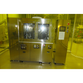
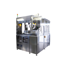
We have compiled a list of manufacturers, distributors, product information, reference prices, and rankings for Developing device.
ipros is IPROS GMS IPROS One of the largest technical database sites in Japan that collects information on.

Developing device Product List and Ranking from 20 Manufacturers, Suppliers and Companies

Last Updated: Aggregation Period:Jul 30, 2025~Aug 26, 2025
This ranking is based on the number of page views on our site.

Developing device Manufacturer, Suppliers and Company Rankings

Last Updated: Aggregation Period:Jul 30, 2025~Aug 26, 2025
This ranking is based on the number of page views on our site.

  1. エイ・エス・エイ・ピイ Saitama//Electronic Components and Semiconductors
  2. null/null
  3. 東京エレクトロン九州 Kumamoto//Electronic Components and Semiconductors
  4. 4 null/null
  5. 5 二宮システム Osaka//others

Developing device Product ranking

Last Updated: Aggregation Period:Jul 30, 2025~Aug 26, 2025
This ranking is based on the number of page views on our site.

  1. Compact Film Automatic Developing Machine NOVA
  2. Tokyo Electron Kyushu Product Catalog 東京エレクトロン九州
  3. Automatic photoresist coating and developing equipment (coater-developer) エイ・エス・エイ・ピイ
  4. 4 Research and development small-sized developing device HPD40 二宮システム
  5. 4 Static development type (paddle) automatic photoresist development device (developer) エイ・エス・エイ・ピイ

Developing device Product List

1~15 item / All 51 items

Displayed results

Development device "GX-40D"

A developing device that is easy to operate with a color LCD touch panel!

The "GX-40D" is a developing device that employs eight nozzle pipes, four on the top and four on the bottom, each capable of individual pressure adjustment. It is mainly suitable for applications such as the development of dry film resist and liquid resist in research and development. 【Features】 ■ Eight nozzle pipes on the top and bottom, each with individually adjustable pressure ■ Horizontal nozzle pipe oscillation ■ Easy operation with a color LCD touch panel ■ Automatically adjusts conveyor speed when the processing time for the chemical solution is input ■ Convenient height for side tank and drain port for easy handling of chemical solutions *For more details, please download the PDF or feel free to contact us.

  • Circuit board processing machine

Added to bookmarks

Bookmarks list

Bookmark has been removed

Bookmarks list

You can't add any more bookmarks

By registering as a member, you can increase the number of bookmarks you can save and organize them with labels.

Free membership registration

Research and development small-sized developing device HPD40

Small Development Printing Device for Research and Development HPD40

【Process】Input → Development → Liquid Cutting → Water Wash 1 → Water Wash 2 → Squeezing → Extraction 【Substrate Size】Max. W400×L500mm Thickness 0.4〜2.0mm 【Nozzle Swing】Horizontal Swing 【Device Size】W1420×L1950×H1645mm - Space-saving for research - Ideal for material development and testing - Capable of developing PCBs and LCDs

  • Other surface treatment equipment
  • Circuit board processing machine
  • Other laboratory equipment and containers

Added to bookmarks

Bookmarks list

Bookmark has been removed

Bookmarks list

You can't add any more bookmarks

By registering as a member, you can increase the number of bookmarks you can save and organize them with labels.

Free membership registration

Small Developer Machine SP Series SPD40

A design that combines user-friendly features with a sleek appearance.

The compact design ultra-high precision series SPseries SPD40 is a small developer that meets the needs for finer printed circuit boards as density increases. It is the definitive compact machine completed by utilizing the know-how of the Ninomiya system, including nozzle, nozzle arrangement, and oscillation. It features user-friendly functions and a sleek design with touch panel operation. Equipped with numerous safety features as standard, it allows for design modifications to meet customer needs. For more details, please contact us or refer to the catalog.

  • Other semiconductor manufacturing equipment

Added to bookmarks

Bookmarks list

Bookmark has been removed

Bookmarks list

You can't add any more bookmarks

By registering as a member, you can increase the number of bookmarks you can save and organize them with labels.

Free membership registration

Liftoff (Image Reversal) Compatible Photoresist Development Equipment

Proven results with a variety of chemical solutions! The reason for our low prices is that we handle everything in-house, from design to sales.

The product is equipped with sheet-type development, front exposure (reverse exposure), baking, and cooling functions. We offer a lineup tailored to production volume, ranging from manual machines to fully automatic machines, and since we handle everything from design to manufacturing and sales in-house, we have achieved low prices. We have a proven track record with a variety of chemicals, including TMAH. 【Features】 ■ Achieves low prices ■ Automatic size recognition ■ Proven track record with a variety of chemicals ■ Reduced footprint ■ Lineup tailored to production volume *For more details, please refer to the PDF document or feel free to contact us.

  • Resist Device

Added to bookmarks

Bookmarks list

Bookmark has been removed

Bookmarks list

You can't add any more bookmarks

By registering as a member, you can increase the number of bookmarks you can save and organize them with labels.

Free membership registration

1 Fluid Spray Type Automatic Photoresist Developer

It is a single-fluid developing device that is effective in reducing the development and processing time of thick films. You can freely choose the spray shape (circular, fan, etc.), pressure, and flow rate.

It is a single-fluid spray-type developing device. Since the spray is generated by the pressure of the developing solution, mist from the spray is less likely to scatter, and it can also speed up the developing process. It is optimal for developing large substrates and thick films. The spray nozzle can be freely selected in terms of shape (such as fan-shaped or circular), distribution, spreading angle, and range. This product is equipped with developing, baking, and cooling functions in a sheet-fed format. With a lineup tailored to production volume, ranging from manual machines to fully automatic machines, we have achieved low prices by handling everything from design to manufacturing and sales in-house. We have a proven track record with a variety of chemicals, including TMAH. 【Features】 ■ Equipped with single-fluid spray (can be used in conjunction with paddles) ■ Automatic wafer size recognition ■ Reduced footprint ■ Lineup tailored to production volume We have a demo setup available, so please consider scheduling a demonstration!

  • Resist Device

Added to bookmarks

Bookmarks list

Bookmark has been removed

Bookmarks list

You can't add any more bookmarks

By registering as a member, you can increase the number of bookmarks you can save and organize them with labels.

Free membership registration

2-fluid spray type automatic photoresist developing device (developer)

From high pressure to mist-like soft pressure, it's all under control! A two-fluid spray resist development device. It is effective in shortening the development time for thick films and more.

This is a developing device that uses a two-fluid spray method to mix and discharge N2 and developer solution. By changing the pressure of N2, the discharge pressure of the spray can be adjusted. You can choose from a wide range of spray discharge patterns, such as increasing the liquid pressure for high-pressure discharge or reducing the liquid volume to create a fine mist for a softer discharge. The spray nozzle can be freely selected in various shapes such as fan-shaped or circular, as well as the distribution, spread angle, and range. We offer a lineup that matches production volume, from manual to fully automatic machines, and since we handle everything from design to manufacturing and sales in-house, we have achieved low prices. We have a proven track record with various chemicals, including TMAH. 【Features】 ■ Equipped with a two-fluid spray! (Paddle can also be used) ■ Automatic wafer size recognition function ■ Proven track record with various chemicals ■ Compact design ■ Lineup tailored to production volume We have a permanent demo setup, so please consider scheduling a demonstration!

  • Resist Device

Added to bookmarks

Bookmarks list

Bookmark has been removed

Bookmarks list

You can't add any more bookmarks

By registering as a member, you can increase the number of bookmarks you can save and organize them with labels.

Free membership registration

Static development type (paddle) automatic photoresist development device (developer)

We have a proven track record with a variety of chemical solutions! The reason for our low prices is that we handle everything in-house, from design to sales.

The development is performed by pooling the developer solution on the wafer in a batch process. Unlike the dip method, each wafer is developed individually, resulting in very high reproducibility of the process. By optimizing the amount of chemical used, it leads to a reduction in the amount of developer solution used. We can accommodate requests for pooling methods, from shower types to straight nozzles. It also features a shaking function during static development! (It moves the liquid by repeating low rotation and stopping.) The batch process includes development, rinsing, baking, and cooling functions. We design, manufacture, and sell according to customer needs and production volumes. We have a proven track record with various chemicals, including TMAH. 【Features】 ■ High reproducibility of development results ■ Reduction in chemical usage ■ Automatic wafer size recognition ■ Proven track record with various chemicals ■ Reduced footprint ■ Design tailored to production volume We have a permanent demo setup, so please consider a demonstration!

  • Resist Device

Added to bookmarks

Bookmarks list

Bookmark has been removed

Bookmarks list

You can't add any more bookmarks

By registering as a member, you can increase the number of bookmarks you can save and organize them with labels.

Free membership registration

Automatic photoresist coating and developing equipment (coater-developer)

Compatible with low to high viscosity resists! We can manufacture equipment for any wafer size, from small diameter to large diameter!

【Features】 ■ Achieves low price ■ Supports low to high viscosity (1.7cP to 10000cP) ■ Compatible with sizes from 2 to 12 inches ■ Capable of processing multiple wafer sizes (e.g., compatible with 3, 4, 5 inches and 8, 12 inches) ■ Automatic wafer size recognition system ■ Proven performance with a variety of chemicals ■ Reduced footprint (space-saving) ■ Numerous options available with resist reduction ■ Lineup tailored to production volume 【ASAP Coater/Developer Functions】 ● Spin coating ● HMDS treatment ● Baking ● Cooling ● Developing ● Rinsing We have achieved low prices by handling everything from design to manufacturing and sales in-house! 【ASAP Features and Achievements】 ● Proven use of a variety of chemicals including positive and negative resists, polyimide, SOG, WAX, silicone, etc. ● Extensive experience in substrate transport including Si (silicon), GaAs, InP, GaN, SiC, sapphire, ceramics, SiO2 (glass), etc. ● Numerous transport achievements with thin substrates such as GaAs (thickness 150um), InP (thickness 150um), LT (thickness 120um)! *For more details, please refer to the PDF document or feel free to contact us.

  • Coater
  • Resist Device
  • Other semiconductor manufacturing equipment

Added to bookmarks

Bookmarks list

Bookmark has been removed

Bookmarks list

You can't add any more bookmarks

By registering as a member, you can increase the number of bookmarks you can save and organize them with labels.

Free membership registration

Small developing device

A small tabletop type spin developer that can perform spray and paddle development.

We have options available according to your budget and usage. Custom products are also available upon request.

  • Resist Device
  • Other semiconductor manufacturing equipment

Added to bookmarks

Bookmarks list

Bookmark has been removed

Bookmarks list

You can't add any more bookmarks

By registering as a member, you can increase the number of bookmarks you can save and organize them with labels.

Free membership registration

Organic solvent-based spray developing device WSD-150

Device dimensions: 560W × 850D × 1300H

Set the substrate in the chuck manually, then perform spray development, rinsing, and spin drying.

  • Other semiconductor manufacturing equipment

Added to bookmarks

Bookmarks list

Bookmark has been removed

Bookmarks list

You can't add any more bookmarks

By registering as a member, you can increase the number of bookmarks you can save and organize them with labels.

Free membership registration

Single-sheet spin developing machine WSD-200CBT/WSD-300CBT

Device dimensions: 1200W × 1100D × 2000H (200CBT) / 1500W × 1100D × 2000H (300CBT)

Set the substrate in the chuck manually, then perform paddle development, rinsing, and spin drying.

  • Other semiconductor manufacturing equipment

Added to bookmarks

Bookmarks list

Bookmark has been removed

Bookmarks list

You can't add any more bookmarks

By registering as a member, you can increase the number of bookmarks you can save and organize them with labels.

Free membership registration

Semiconductor printed circuit board horizontal manufacturing equipment for solder resist development (finishing process)

Supports everything from single-layer substrates to flexible substrates using Roll to Roll! No resist residue remains.

We would like to introduce the solder resist development for finishing treatment handled by Fujikiko Co., Ltd. It accommodates everything from single-sided PCBs to flexible PCBs using Roll to Roll. Additionally, due to optimal spray placement, there is no residue left from the resist. 【Features】 ■ Accommodates everything from single-sided PCBs to flexible PCBs using Roll to Roll ■ Optimal spray placement ■ No resist residue left *For more details, please refer to the PDF document or feel free to contact us.

  • Other semiconductor manufacturing equipment
  • Other surface treatment equipment
  • Circuit board processing machine

Added to bookmarks

Bookmarks list

Bookmark has been removed

Bookmarks list

You can't add any more bookmarks

By registering as a member, you can increase the number of bookmarks you can save and organize them with labels.

Free membership registration