
List of Semiconductor Manufacturing Equipment products
- classification:Semiconductor Manufacturing Equipment
136~180 item / All 5250 items


It won't break even after 1 million repetitions! A mat switch with reliable operation, high durability, and low price. Suitable for options in machine tools as well. Please consult us about delivery t...
- Sensors


We can accommodate high resistance over 10,000 ohms, with diameters ranging from approximately 30 mm to 8 inches, and we also offer thinning and chip processing arrangements!
- Other semiconductors
- Processing Contract
- Wafer


Achieving high-quality polishing that preserves the edge through automation.
- Wafer processing/polishing equipment

We will exhibit at the SURTECH 2025 trade show.
We will be exhibiting at SURTECH 2025 – Surface Technology Exhibition – which will be held at Tokyo Big Sight from January 29, 2025 (Wednesday). We will introduce the "DLyte," a dry electrochemical polishing machine that uses resin media for ion exchange to grind and polish metals. Exhibition: SURTECH 2025 Location: Tokyo Big Sight, East Hall 3 Organizer: JTB Communication Design, Inc. (Rapid News Publications Ltd.) Date: January 29 (Wednesday) to January 31 (Saturday), 2025 Time: 10:00 AM to 5:00 PM Booth Number: 3X-11 *For inquiries and to download the catalog, please visit here. You can find more detailed information on our website. Request for materials: https://www.nttdata-xam.com/document/ Inquiries: https://www.nttdata-xam.com/contact/

Achieving high-quality polishing that preserves edges through mechanization.
- Wafer processing/polishing equipment
We will exhibit at the SURTECH 2025 trade show.
We will be exhibiting at SURTECH 2025 – Surface Technology Exhibition – which will be held at Tokyo Big Sight from January 29, 2025 (Wednesday). We will introduce the "DLyte," a dry electrochemical polishing machine that uses resin media for ion exchange to grind and polish metals. Exhibition: SURTECH 2025 Location: Tokyo Big Sight, East Hall 3 Organizer: JTB Communication Design, Inc. (Rapid News Publications Ltd.) Date: January 29 (Wednesday) to January 31 (Saturday), 2025 Time: 10:00 AM to 5:00 PM Booth Number: 3X-11 *For inquiries and to download the catalog, please visit here. You can find more detailed information on our website. Request for materials: https://www.nttdata-xam.com/document/ Inquiries: https://www.nttdata-xam.com/contact/

Achieving high-quality polishing that retains the edge through mechanization.
- Wafer processing/polishing equipment
We will exhibit at the SURTECH 2025 trade show.
We will be exhibiting at SURTECH 2025 – Surface Technology Exhibition – which will be held at Tokyo Big Sight from January 29, 2025 (Wednesday). We will introduce the "DLyte," a dry electrochemical polishing machine that uses resin media for ion exchange to grind and polish metals. Exhibition: SURTECH 2025 Location: Tokyo Big Sight, East Hall 3 Organizer: JTB Communication Design, Inc. (Rapid News Publications Ltd.) Date: January 29 (Wednesday) to January 31 (Saturday), 2025 Time: 10:00 AM to 5:00 PM Booth Number: 3X-11 *For inquiries and to download the catalog, please visit here. You can find more detailed information on our website. Request for materials: https://www.nttdata-xam.com/document/ Inquiries: https://www.nttdata-xam.com/contact/

Achieving high-quality polishing that preserves edges through mechanization.
- Wafer processing/polishing equipment
We will exhibit at the SURTECH 2025 trade show.
We will be exhibiting at SURTECH 2025 – Surface Technology Exhibition – which will be held at Tokyo Big Sight from January 29, 2025 (Wednesday). We will introduce the "DLyte," a dry electrochemical polishing machine that uses resin media for ion exchange to grind and polish metals. Exhibition: SURTECH 2025 Location: Tokyo Big Sight, East Hall 3 Organizer: JTB Communication Design, Inc. (Rapid News Publications Ltd.) Date: January 29 (Wednesday) to January 31 (Saturday), 2025 Time: 10:00 AM to 5:00 PM Booth Number: 3X-11 *For inquiries and to download the catalog, please visit here. You can find more detailed information on our website. Request for materials: https://www.nttdata-xam.com/document/ Inquiries: https://www.nttdata-xam.com/contact/

Achieving high-quality polishing that preserves the edge through mechanization.
- Wafer processing/polishing equipment
We will exhibit at the SURTECH 2025 trade show.
We will be exhibiting at SURTECH 2025 – Surface Technology Exhibition – which will be held at Tokyo Big Sight from January 29, 2025 (Wednesday). We will introduce the "DLyte," a dry electrochemical polishing machine that uses resin media for ion exchange to grind and polish metals. Exhibition: SURTECH 2025 Location: Tokyo Big Sight, East Hall 3 Organizer: JTB Communication Design, Inc. (Rapid News Publications Ltd.) Date: January 29 (Wednesday) to January 31 (Saturday), 2025 Time: 10:00 AM to 5:00 PM Booth Number: 3X-11 *For inquiries and to download the catalog, please visit here. You can find more detailed information on our website. Request for materials: https://www.nttdata-xam.com/document/ Inquiries: https://www.nttdata-xam.com/contact/
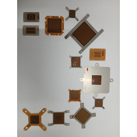

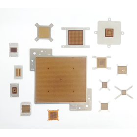
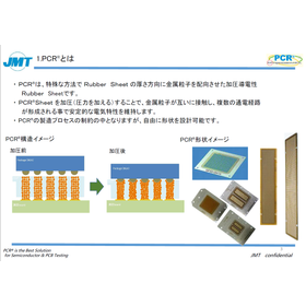
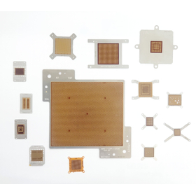
A sheet socket that enables stable inspection in semiconductor back-end process inspection! What is "PCR" that allows for high-speed and high-density measurements? Technical materials on operating pri...
- Other electronic parts
- socket
- Semiconductor inspection/test equipment

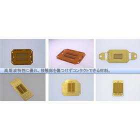
Test solution that does not damage solder balls or measurement substrates with soft contact!
- Semiconductor inspection/test equipment
- Printed Circuit Board


Maximum operating temperature 2000℃ Semi-automatic control Ultra-high temperature experimental furnace (carbon furnace, tungsten metal furnace) Compact and space-saving experimental furnace
- Heating device
- Annealing furnace
- Electric furnace

VOXIA compact X-ray CT imaging device
Compact design with a space-saving layout that can be installed anywhere. Despite its compact body, it generates high-resolution data through advanced calculation software. * X-ray tube voltage: 20-90kV, or 40-maximum 130kV * Focus diameter: 7μm (5μm@4W) * Detector pixel: 89μm, approximately 3.2 million pixels! * Sample size: Φ120mm ◉ Vcap (Control Software): A custom-made imaging stage tailored to the subject and purpose. A series of tasks from shooting to image output can be performed with just a click. High-speed continuous shooting in as fast as 20 seconds, with processing from shooting start to image reconstruction taking about 30 seconds. ◉ VCT (Reconstruction Software): Customizable automatic measurement and analysis software specialized for the specified subject. High-speed reconstruction of shooting data with 992 x 992 pixel images and 600 projections in just 3.8 seconds! ◉ MolcerPlus (3D Display Analysis): Custom software that enables measurement conditions that were difficult with conventional software. Software for displaying, processing, and measuring the imaged object. ● High safety, ● Compatible with a wide variety of samples, ● Intuitive HMI, easy operation.

Maximum operating temperature 2000℃ Semi-automatic control Ultra-high temperature experimental furnace (carbon furnace, tungsten metal furnace) Compact and space-saving experimental furnace
- Heating device
- Annealing furnace
- Electric furnace

Multi-Target Sputtering Device [MiniLab-125] Compatible with Φ8" SiC Coating Equipped with 1000℃ Heater Stage! Compact Size!
Multifunctional Multi-Sputtering Device (Compatible with Φ8inch Substrates) - Simultaneous deposition of three components + one component Pulse DC sputtering - Flexible arrangement of RF500W and DC850W power supplies to three cathodes (Source 1, 2, 3) - Equipped with a 5KW Pulse DC power supply → used with dedicated cathode (4) - Substrate heating stage Max 800℃ (SiC coated heater can achieve Max 1000℃) - MFC x 3 systems (Ar, O2, N2) for reactive sputtering - Main chamber RIE etching stage RF300W - LL chamber <30W low power controlled soft etching - Unique "Soft-Etching" technology reduces substrate damage through substrate bias - Touch panel or Windows PC operation: All operations can be performed on the touch panel/PC without dispersing control. - Equipment installation dimensions: 1,960(W) x 1,100(D) x 1,700(H) mm - Multi-chamber type can also be manufactured. ● Mixed specifications for resistance heating deposition, organic material deposition, EB deposition, PECVD, etc. are also possible.
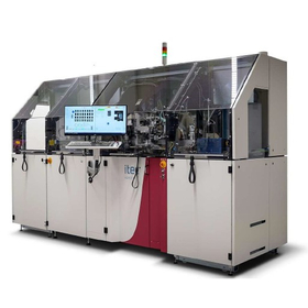

A method to triple production capacity without expanding the clean room!
- Bonding Equipment
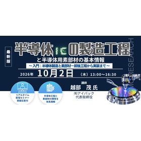

A systematic explanation of the manufacturing process of semiconductor ICs, from the front-end and back-end processes to assembly, including the roles and necessity of the materials used in each stage...
- Other semiconductors
- Other semiconductor manufacturing equipment
- Technical Seminar

Due to its modular embedded design, it is possible to flexibly assemble dedicated equipment according to the required film formation method. A compact thin-film experimental device that can accommodat...
- Sputtering Equipment
VOXIA compact X-ray CT imaging device
Compact design with a space-saving layout that can be installed anywhere. Despite its compact body, it generates high-resolution data through advanced calculation software. * X-ray tube voltage: 20-90kV, or 40-maximum 130kV * Focus diameter: 7μm (5μm@4W) * Detector pixel: 89μm, approximately 3.2 million pixels! * Sample size: Φ120mm ◉ Vcap (Control Software): A custom-made imaging stage tailored to the subject and purpose. A series of tasks from shooting to image output can be performed with just a click. High-speed continuous shooting in as fast as 20 seconds, with processing from shooting start to image reconstruction taking about 30 seconds. ◉ VCT (Reconstruction Software): Customizable automatic measurement and analysis software specialized for the specified subject. High-speed reconstruction of shooting data with 992 x 992 pixel images and 600 projections in just 3.8 seconds! ◉ MolcerPlus (3D Display Analysis): Custom software that enables measurement conditions that were difficult with conventional software. Software for displaying, processing, and measuring the imaged object. ● High safety, ● Compatible with a wide variety of samples, ● Intuitive HMI, easy operation.


Are you having trouble with the delivery time for cast prototypes? "Casting prototype service!" for cast iron, aluminum castings, and stainless steel castings (lost wax casting)!
- Other semiconductor manufacturing equipment
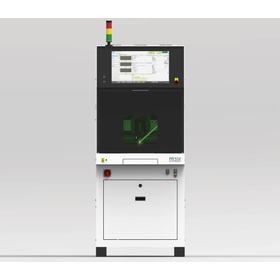

Easier wedge bonding of copper wire using heating technology.
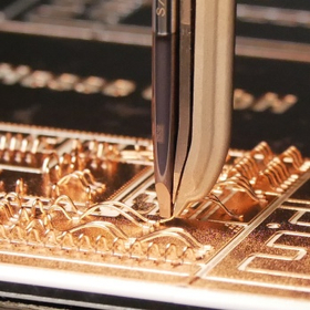
- Bonding Equipment
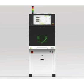
Easily connect copper wire chips with innovative laser heating.
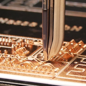
- Bonding Equipment
The optimal bonding solution for the aerospace field, which requires high reliability.
- Bonding Equipment
High-precision bonding solutions that meet miniaturization needs.
- Bonding Equipment
Providing the optimal bond for high-brightness LED manufacturing.
- Bonding Equipment
Providing optimal and high-quality bonds that correspond to high currents.
- Bonding Equipment
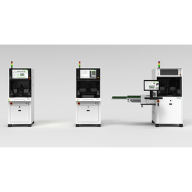
Achieving high-quality bonds optimized for automotive powertrains.
- Bonding Equipment
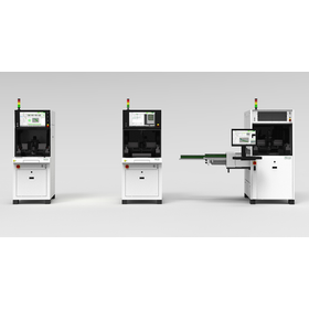
Reliable bonding solutions that support the robustness of industrial robots.
- Bonding Equipment
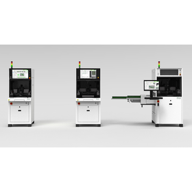
Bonding solutions that contribute to improving productivity and reducing costs in home appliance manufacturing.
- Bonding Equipment
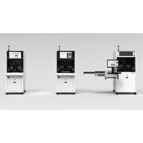
Providing optimal and high-quality bonding that supports multi-pin configurations.
- Bonding Equipment
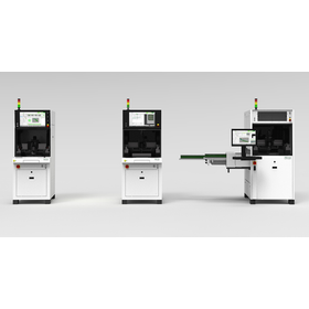
Providing the ideal bond for manufacturing high-sensitivity sensors.
- Bonding Equipment
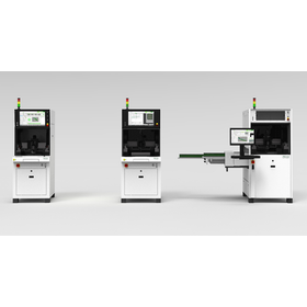
Providing bonds that contribute to improving durability in the renewable energy sector.
- Bonding Equipment
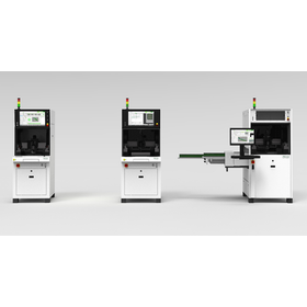
Providing optimal and high-quality bonds that support high-speed transmission.
- Bonding Equipment
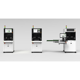
Providing optimal adhesive for large-capacity bonding for EV batteries.
- Bonding Equipment

Bond head replacement completed in a few minutes! Compatible with ball bonding, fine wire, and thick wire, etc.
- Bonding Equipment
![Soft Etching Device [nanoETCH]](https://image.mono.ipros.com/public/product/image/e80/2000071234/IPROS34856758710167043703.jpeg?w=280&h=280)
<30W Low power - Etching control precision 10mW Achieving damage-free and delicate etching processing.
- Etching Equipment
VOXIA compact X-ray CT imaging device
Compact design with a space-saving layout that can be installed anywhere. Despite its compact body, it generates high-resolution data through advanced calculation software. * X-ray tube voltage: 20-90kV, or 40-maximum 130kV * Focus diameter: 7μm (5μm@4W) * Detector pixel: 89μm, approximately 3.2 million pixels! * Sample size: Φ120mm ◉ Vcap (Control Software): A custom-made imaging stage tailored to the subject and purpose. A series of tasks from shooting to image output can be performed with just a click. High-speed continuous shooting in as fast as 20 seconds, with processing from shooting start to image reconstruction taking about 30 seconds. ◉ VCT (Reconstruction Software): Customizable automatic measurement and analysis software specialized for the specified subject. High-speed reconstruction of shooting data with 992 x 992 pixel images and 600 projections in just 3.8 seconds! ◉ MolcerPlus (3D Display Analysis): Custom software that enables measurement conditions that were difficult with conventional software. Software for displaying, processing, and measuring the imaged object. ● High safety, ● Compatible with a wide variety of samples, ● Intuitive HMI, easy operation.
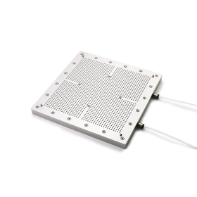

For correcting and fixing the warping of films, wafers, and thin plates. Choose from 3 methods × 60 standard types.
- Other semiconductor manufacturing equipment
- Visual Inspection Equipment
- Other machine elements

Compact and space-saving! Ideal for research and development. Flexible configuration for purposes such as deposition, sputtering, and annealing.
- Evaporation Equipment
- Sputtering Equipment
- Annealing furnace
VOXIA compact X-ray CT imaging device
Compact design with a space-saving layout that can be installed anywhere. Despite its compact body, it generates high-resolution data through advanced calculation software. * X-ray tube voltage: 20-90kV, or 40-maximum 130kV * Focus diameter: 7μm (5μm@4W) * Detector pixel: 89μm, approximately 3.2 million pixels! * Sample size: Φ120mm ◉ Vcap (Control Software): A custom-made imaging stage tailored to the subject and purpose. A series of tasks from shooting to image output can be performed with just a click. High-speed continuous shooting in as fast as 20 seconds, with processing from shooting start to image reconstruction taking about 30 seconds. ◉ VCT (Reconstruction Software): Customizable automatic measurement and analysis software specialized for the specified subject. High-speed reconstruction of shooting data with 992 x 992 pixel images and 600 projections in just 3.8 seconds! ◉ MolcerPlus (3D Display Analysis): Custom software that enables measurement conditions that were difficult with conventional software. Software for displaying, processing, and measuring the imaged object. ● High safety, ● Compatible with a wide variety of samples, ● Intuitive HMI, easy operation.

It is a high-performance vacuum deposition source that can be used as a high-temperature heating cell for vacuum applications, with an organic deposition source up to 800°C and a metal deposition sour...
- Evaporation Equipment
- Heating device
- Electric furnace
VOXIA box X-ray CT imaging device
Compact design with a space-saving layout that can be installed anywhere. Despite its compact body, it generates high-resolution data through advanced calculation software. * X-ray tube voltage: 0–150kV * Focus diameter: 7μm (5μm@4W) * Detector pixel: 49.5μm, 6.75 million pixels! * Sample size: Φ100mm ◉ Vcap (control software): A custom-made imaging stage tailored to the subject and purpose. A series of tasks from shooting to image output can be performed with just a click. High-speed continuous shooting in as fast as 20 seconds, with processing from shooting start to image reconstruction taking about 30 seconds. ◉ VCT (reconstruction software): Customizable automatic measurement and analysis software specialized for the specified subject. High-speed reconstruction of shooting data with an image size of 992 x 992 pixels and 600 projections in just 3.8 seconds! ◉ MolcerPlus (3D display analysis): Custom software that enables measurement conditions that were difficult with conventional software. Software for displaying, processing, and measuring the imaged object. ● High safety, ● Compatible with a wide variety of samples, ● Intuitive HMI, easy operation.

Wide range of support from surface-treated steel plates to heavy processing! Combinations of polishing brushes, polishing wheels, vertical brushes, and wire brushes are available for selection.
- Wafer processing/polishing equipment
- Other abrasives
- Other surface treatment equipment


Resist coater for cover glass integrated touch panel (OGS)
- Resist Device

A 3D spray coater that can be applied to any 3D shape. It reads the substrate shape with a laser scanner and automatically generates the application path.
- Coater

High-precision spray coater designed for developers for process development of various nano materials such as touch panels and fuel cells!
- Coater


An electrical characteristic testing system that maximizes the performance of power devices for EV control.
- Tester
- Semiconductor inspection/test equipment
- Testing Equipment and Devices

SPEA DOT800T Electrical Characteristic Testing System for Power Devices
- Tester
- Semiconductor inspection/test equipment
- Testing Equipment and Devices
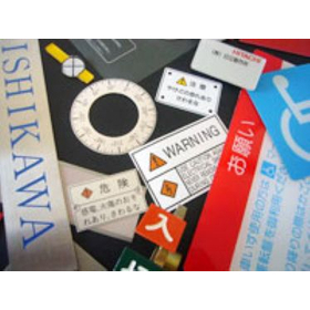

We will solve the shortage of outsourcing partners for precision processing due to capacity overload at existing factories, such as in semiconductors and precision components.
- Etching Equipment
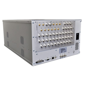

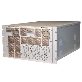
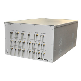
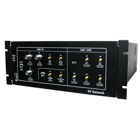
We aim to support our customers in mastering all aspects of their maintenance strategy!
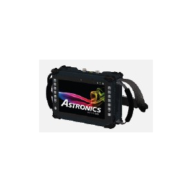
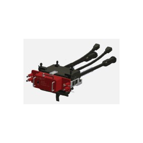
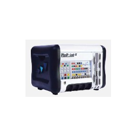
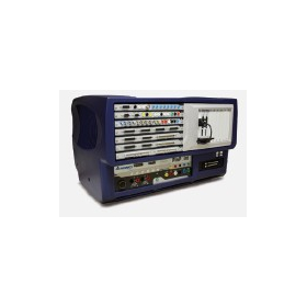
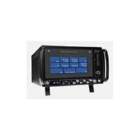
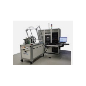
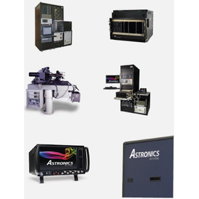
- Tester