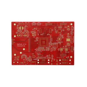
We have compiled a list of manufacturers, distributors, product information, reference prices, and rankings for substrate.
ipros is IPROS GMS IPROS One of the largest technical database sites in Japan that collects information on.

substrate Product List and Ranking from 576 Manufacturers, Suppliers and Companies | IPROS GMS

Last Updated: Aggregation Period:Jul 22, 2026~Aug 18, 2026
This ranking is based on the number of page views on our site.

substrate Manufacturer, Suppliers and Company Rankings

Last Updated: Aggregation Period:Jul 22, 2026~Aug 18, 2026
This ranking is based on the number of page views on our site.

  1. スクリーンプロセス Kanagawa//others
  2. 太洋テクノレックス 本社 和歌山 Wakayama//Electronic Components and Semiconductors
  3. 共立エレックス Saga//Ceramics
  4. 4 山下マテリアル Kanagawa//Electronic Components and Semiconductors
  5. 5 アイン 本社工場 Nagano//Electronic Components and Semiconductors

substrate Product ranking

Last Updated: Aggregation Period:Jul 22, 2026~Aug 18, 2026
This ranking is based on the number of page views on our site.

  1. <Super Short Delivery Time> Base Material Specification Sheet スクリーンプロセス
  2. Ceramic substrate for firing setters 共立エレックス
  3. Long-sized printed circuit board ☆ up to 1500mm ☆ Ally Japan 横浜本社
  4. 4 PICLIA Ribbon Dual Sensor (Piezoelectric & Capacitive) *Evaluation Kit DAIKIN FINETECH, LTD.
  5. 5 Wrist Frequency Correction Vibration Acceleration Effective Value Measuring Instrument 'TVHP-001' 吉川電機製作所

substrate Product List

511~540 item / All 1969 items

Displayed results

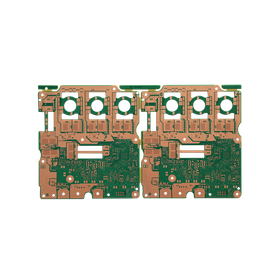
End face through-hole substrate. Our unique processing solves copper burrs and powder drop!

We will solve the implementation issues and challenges arising from the miniaturization of electronic components with our special structures such as edge-through-hole boards and laminated boards.

End face through holes are formed by cutting through holes created at the edges of the substrate using contour processing. Traditionally, copper burrs were generated during the cutting of through holes, but our company can provide end face through holes without burrs even with router processing thanks to our unique process. Additionally, this unique process allows for the partial etching of landless through holes and the copper plating of through holes. In printed circuit boards for electronic device applications such as compact modules, miniaturization and heat dissipation are required. Our company offers special structure printed circuit boards tailored to your needs, such as metal cavity structure boards and three-dimensional structure boards through lamination.

  • Circuit board design and manufacturing
  • substrate

Added to bookmarks

Bookmarks list

Bookmark has been removed

Bookmarks list

You can't add any more bookmarks

By registering as a member, you can increase the number of bookmarks you can save and organize them with labels.

Free membership registration

MI-PCB Technology

High heat dissipation and noise issue resolution with GND reinforcement MI-PCB technology!

"MI-PCB Technology" is a new concept PCB technology that aims to efficiently solve problems by inserting thick metals with excellent thermal conductivity at appropriate positions within the PCB layers. It possesses Thick Metal Etching & Patterning Technology. It can be used in automotive products, electric vehicles, smartphones, and more. 【Features】 ■ High Thermal Performance ■ Reduces the thickness of electronic product sets ■ No need for heatsinks ■ Eliminates processes related to heatsink attachment, improving productivity (No need for thermal grease application and eliminates the heatsink attachment process) *For more details, please refer to the PDF document or feel free to contact us.

Added to bookmarks

Bookmarks list

Bookmark has been removed

Bookmarks list

You can't add any more bookmarks

By registering as a member, you can increase the number of bookmarks you can save and organize them with labels.

Free membership registration

Heat-dissipating substrate "DPGA"

This is a substrate with unique high heat dissipation properties developed by Daiwa Kogyo Co., Ltd.

"DPGA" stands for "Daiwa Process Global Advance," which is a process developed independently by Daiwa Industrial that uses metal Cu bumps for interlayer wiring connections. A substrate with high heat dissipation characteristics enables high brightness and long lifespan of LEDs, as well as miniaturization of heat sinks. 【Features】 ○ Interlayer connection using metal pillars (copper bumps) → Achieves low resistance, high connection reliability, and high thermal conductivity ○ Copper bumps can be of any shape and size → For cylindrical shapes, diameters can range from 0.3 to 4.00 mm ○ Mixing of copper bumps of different sizes is possible ○ Improved thinness, lightness, and rigidity → Minimum board thickness: 0.3 mm, using prepreg for the insulation layer ○ Maximizes the functionality of LEDs → Ideal for LED substrates (liquid crystal panels, lighting) and automotive substrates For more details, please contact us or download the catalog.

  • Printed Circuit Board
  • substrate

Added to bookmarks

Bookmarks list

Bookmark has been removed

Bookmarks list

You can't add any more bookmarks

By registering as a member, you can increase the number of bookmarks you can save and organize them with labels.

Free membership registration

Cost reduction: High heat dissipation, high current circuit board

Achieving unit cost reduction, unit size reduction, and extended lifespan. Ideal for LED substrates and automotive substrates!

We would like to introduce Daiwa Kogyo Co., Ltd.'s "High Heat Dissipation and High Current Circuit Boards." Our "High Heat Dissipation Circuit Board" replaces ceramic substrates, achieving cost reduction in substrate expenses. Additionally, by switching from water cooling to air cooling, we achieve cost reduction in unit expenses. We also manufacture products such as "Copper Pin Embedded Circuit Boards," which reduce thermal damage to components, as well as "Aluminum Base/Copper Base Circuit Boards" that can handle thermal conductivity up to 10W, and "Thick Copper Circuit Boards" suitable for high current. If you are having trouble with circuit boards, please feel free to consult with us. 【Features】 ■ High Heat Dissipation Circuit Board - Achieves cost reduction in substrate expenses by replacing ceramic substrates - Achieves cost reduction in unit expenses by switching from water cooling to air cooling - Realizes reduction in unit size and component costs through miniaturization of heat sinks/fans ■ Copper Pin Embedded Circuit Board - Provides pinpoint heat dissipation from high-heat components - Reduces thermal damage to components *For more details, please refer to the PDF document or feel free to contact us.

  • Printed Circuit Board
  • Circuit board design and manufacturing
  • substrate

Added to bookmarks

Bookmarks list

Bookmark has been removed

Bookmarks list

You can't add any more bookmarks

By registering as a member, you can increase the number of bookmarks you can save and organize them with labels.

Free membership registration

Daiwa Industrial Co., Ltd. Company Profile

Addressing environmental issues! We provide customers with excitement and satisfaction through manufacturing and technology development.

Our company was founded in 1967, starting as a metal pressing processing business, and applied that technology to the contour processing of printed circuit boards. We began manufacturing printed circuit boards in 1982 and have continued to this day. We have also succeeded in developing technology that enables general printed circuit boards to have heat dissipation properties equivalent to or exceeding those of ceramics. Focusing on "manufacturing and technology development" that leads the world without being swayed by environmental changes, we provide our customers with excitement and satisfaction. 【Business Activities】 ■ Manufacturing, development, and sales of printed wiring boards *For more details, please refer to the PDF document or feel free to contact us.

  • Wiring materials
  • Contract manufacturing
  • Circuit board design and manufacturing
  • substrate

Added to bookmarks

Bookmarks list

Bookmark has been removed

Bookmarks list

You can't add any more bookmarks

By registering as a member, you can increase the number of bookmarks you can save and organize them with labels.

Free membership registration

High Heat Dissipation Substrate 'DPGA-M'

DPGA is made double-sided and supports back-side wiring! Equal-length wiring is possible even when parallel circuits are present.

"DPGA-M" is a high thermal conductivity substrate that features a single-sided multilayer design and supports backside wiring. By adopting a single-sided multilayer structure, it significantly enhances design flexibility, allowing for backside wiring. Although it has multiple layers stacked on one side, it is possible to penetrate copper bumps. This enables direct connection of high thermal conductivity components to the copper base and heat sink. 【Features】 ■ Single-sided multilayer structure ■ Enables backside wiring ■ Allows for equal-length wiring even in the presence of parallel circuits ■ Significantly increases design flexibility ■ Enables direct connection of high thermal conductivity components to the copper base and heat sink *For more details, please refer to the PDF document or feel free to contact us.

  • Circuit board design and manufacturing
  • Printed Circuit Board
  • substrate

Added to bookmarks

Bookmarks list

Bookmark has been removed

Bookmarks list

You can't add any more bookmarks

By registering as a member, you can increase the number of bookmarks you can save and organize them with labels.

Free membership registration

High Heat Dissipation Substrate 'DPGA-S'

Separating the copper base on the back and ensuring insulation! Maintaining the strength of the substrate even after separating the copper base.

The "DPGA-S" is a high thermal conductivity substrate that separates the copper base on the back side and is designed for insulation. Thanks to the high thermal conductivity provided by the through-type copper bumps, it is possible to make the insulation layer up to 0.3mm thick. This allows for maintaining the strength of the substrate even after separating the copper base. Additionally, by separating the layers, it is also possible to mount electrodes on the copper base side. 【Features】 ■ High thermal conductivity due to through-type copper bumps ■ Insulation layer can be made up to 0.3mm thick ■ Allows for mounting electrodes on the copper base side by separating the layers ■ The back side can also be utilized for electrical connections *For more details, please refer to the PDF document or feel free to contact us.

  • Circuit board design and manufacturing
  • Printed Circuit Board
  • substrate

Added to bookmarks

Bookmarks list

Bookmark has been removed

Bookmarks list

You can't add any more bookmarks

By registering as a member, you can increase the number of bookmarks you can save and organize them with labels.

Free membership registration

Copper Pin Embedded Substrate "DPGA-EF"

Embed copper pins directly under the heating components! This can reduce the cost difference based on the number of copper pins.

"DPGA-EF" is a type of substrate that embeds copper pins only in the necessary areas. It can be produced at a lower cost compared to copper bases with bumps. The copper pins are inserted into the holes of the rigid substrate and fixed with resin. Unlike press-fitting, there is no risk of cracks or other issues. Additionally, the copper pins are embedded all at once. Unlike the press-fitting method, the cost difference based on the number of copper pins can be minimized. 【Features】 ■ Both sides of components can be mounted ■ Heat-generating components can be cooled precisely ■ There are no concerns about cracks or chemical residue, as it differs from the copper pin press-fitting method ■ It can be produced at a lower cost compared to copper bases with bumps ■ Unlike the press-fitting method, the cost difference based on the number of copper pins can be minimized *For more details, please refer to the PDF document or feel free to contact us.

  • Circuit board design and manufacturing
  • Printed Circuit Board
  • substrate

Added to bookmarks

Bookmarks list

Bookmark has been removed

Bookmarks list

You can't add any more bookmarks

By registering as a member, you can increase the number of bookmarks you can save and organize them with labels.

Free membership registration

Copper base / aluminum base substrate

The thermal conductivity can support up to 10W! Introducing a single-sided, one-layer metal substrate using a high thermal conductivity insulation layer.

We would like to introduce our "Copper Base/Aluminum Base Substrates." The "Copper Base" is a plain substrate without copper bumps. It features a high thermal conductivity copper material with a 4-10W insulation layer and copper foil laminated together, suitable for high heat dissipation of LEDs. The "Aluminum Base Substrate" is compatible with aluminum substrate materials from various manufacturers. You can choose suitable materials from a wide lineup based on thickness, thermal conductivity, and more. 【Features】 <Copper Base> - No copper bumps - High thermal conductivity copper material with a 4-10W insulation layer and copper foil laminated - Suitable for high heat dissipation of LEDs <Aluminum Base Substrate> - Compatible with aluminum substrate materials from various manufacturers - A wide selection of suitable materials available *For more details, please refer to the PDF document or feel free to contact us.

  • Circuit board design and manufacturing
  • Printed Circuit Board
  • substrate

Added to bookmarks

Bookmarks list

Bookmark has been removed

Bookmarks list

You can't add any more bookmarks

By registering as a member, you can increase the number of bookmarks you can save and organize them with labels.

Free membership registration

High current compatible thick copper substrate

We introduce a thick copper substrate that incorporates a 400μ copper plate bonded to the core material, accommodating multilayer configurations.

The "High Current Compatible Thick Copper Substrate" is a substrate that consists of a core material bonded with a copper plate as the outer layer. The thickness of the outer layer copper can be up to 400μ. It is designed to accommodate high current applications. Additionally, it can also support multilayer boards where copper plates are bonded to the inner layers, with only the outer layer being thick copper. Thick copper can be used for both outer layer circuits and inner layer circuits. 【Features】 ■ A 4-layer board combining 35μ inner layer with 300μ outer layer ■ Compatible with the step of thick copper through silk printing with inkjet *For more details, please refer to the PDF document or feel free to contact us.

  • Circuit board design and manufacturing
  • Printed Circuit Board
  • substrate

Added to bookmarks

Bookmarks list

Bookmark has been removed

Bookmarks list

You can't add any more bookmarks

By registering as a member, you can increase the number of bookmarks you can save and organize them with labels.

Free membership registration

Analog and Digital Circuit Design & Software Production

We have 40 years of experience in analog and digital circuit design and software development, and we are also engaged in new technology development.

We are developing and supplying CPU boards for industrial use using the RX family. This family achieves high computational performance and excellent low power consumption, making it suitable for applications ranging from small-scale to large-scale. We develop products that meet customer needs, from circuit design to prototype mass production, using this CPU.

  • Instrumentation and Control Systems
  • Control Panel
  • substrate

Added to bookmarks

Bookmarks list

Bookmark has been removed

Bookmarks list

You can't add any more bookmarks

By registering as a member, you can increase the number of bookmarks you can save and organize them with labels.

Free membership registration

Maruwa Manufacturing Co., Ltd. Business Introduction

Specialized manufacturer of flexible printed circuit boards (FPC)!

Maruwa Manufacturing Co., Ltd. is a company primarily engaged in the manufacturing and sales of flexible printed circuit boards (FPC). Our products are used in various applications such as space and aerospace equipment, as well as medical devices. To meet diverse needs, we possess advanced technologies for high-density FPC formation and thin FPC formation, and with our extensive experience and production techniques, we provide timely FPC solutions that satisfy our customers. For any inquiries regarding flexible printed circuit boards (FPC), please feel free to consult with us. [Business Activities] ■ Manufacturing and sales of flexible printed circuit boards (FPC) *For more details, please refer to our catalog or feel free to contact us.

  • Other electronic components and modules
  • Other Machine Parts
  • substrate

Added to bookmarks

Bookmarks list

Bookmark has been removed

Bookmarks list

You can't add any more bookmarks

By registering as a member, you can increase the number of bookmarks you can save and organize them with labels.

Free membership registration

FPC "Single-sided FPC"

Ideal for flexible bending and effective use of embedded space!

"Single-sided FPC" is a printed circuit board that has a conductor pattern on only one side. Due to its thinness, it allows for flexible bending and effective use of assembly space, and we also offer fine-pitch specifications in addition to standard specifications. This product is mainly used in backlights and motors. 【Features】 ■ Conductor pattern on one side only ■ Allows for flexible bending and effective use of assembly space *For more details, please refer to the catalog or feel free to contact us.

  • Electronic Components
  • Other Machine Parts
  • substrate

Added to bookmarks

Bookmarks list

Bookmark has been removed

Bookmarks list

You can't add any more bookmarks

By registering as a member, you can increase the number of bookmarks you can save and organize them with labels.

Free membership registration

Japan Universe Co., Ltd. (Printed Circuit Board Division) Company Profile

We provide comprehensive technology related to electronic devices from specification creation to development, design, manufacturing, and evaluation.

At Nippon Universe Co., Ltd. - Printed Circuit Board Division, we utilize the technology we have cultivated over 48 years to respond to printed circuit board design, manufacturing, and assembly with small quantities and short lead times. We are enhancing our simulation technology to aim for higher quality designs. In wiring design, we can significantly shorten design lead times through a simultaneous parallel design system. We support the establishment of ultra-short lead time lines that operate on weekends and holidays, as well as provide assistance from numerous satellite design offices across the country. We also handle the preparation of documentation related to circuit boards and have extensive experience in high-speed signal design (LVDS2, DDR2, DDR3). Regarding manufacturing (outsourcing), we can accommodate short lead times for single-sided boards to 36-layer high multilayer boards, as well as various types of board manufacturing (high multilayer boards, flex, ceramic boards, BGA). We select the optimal factory based on customer requirements (high difficulty, budget, lead time). For component assembly (outsourcing), we can achieve high-quality assembly with the latest equipment (maintaining a defect rate of 0.003 or lower). We respond to short lead times through manual assembly and mounting machines. For more details, please contact us or download our catalog.

  • Circuit board design and manufacturing
  • Printed Circuit Board
  • substrate

Added to bookmarks

Bookmarks list

Bookmark has been removed

Bookmarks list

You can't add any more bookmarks

By registering as a member, you can increase the number of bookmarks you can save and organize them with labels.

Free membership registration

Business Information: Japan Universe Co., Ltd.

We provide comprehensive technology related to electronic devices from specification creation to development, design, manufacturing, and evaluation.

Japan Universe Co., Ltd. provides comprehensive technology related to electronic devices, from specification creation to development, design, manufacturing, and evaluation. We have established an environment that allows for integrated production of everything, enabling high quality along with small lot sizes, a variety of products, and short delivery times. Please feel free to consult with us first. 【Business Content】 ■ Design, manufacturing (outsourcing), assembly (outsourcing), and sales of printed circuit boards ■ Dispatch services *For more details, please refer to the PDF materials or feel free to contact us.

  • Circuit board design and manufacturing
  • Printed Circuit Board
  • substrate

Added to bookmarks

Bookmarks list

Bookmark has been removed

Bookmarks list

You can't add any more bookmarks

By registering as a member, you can increase the number of bookmarks you can save and organize them with labels.

Free membership registration

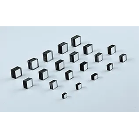
GaN substrate (square)

Gallium nitride (GaN) is a very hard and mechanically stable wide-bandgap semiconductor.

Gallium nitride (GaN) is a very hard and mechanically stable wide-bandgap semiconductor. Due to its higher breakdown voltage, faster switching speed, higher thermal conductivity, and lower on-resistance, GaN-based power devices are significantly superior to silicon-based devices.

  • Other metal materials
  • substrate

Added to bookmarks

Bookmarks list

Bookmark has been removed

Bookmarks list

You can't add any more bookmarks

By registering as a member, you can increase the number of bookmarks you can save and organize them with labels.

Free membership registration

CVD diamond substrate

Diamond substrate, diamond

CVD diamond substrates (Chemical Vapor Deposition diamond substrates) are materials that use thin films of diamond produced by the chemical vapor deposition (CVD) method as a substrate. In the CVD method, diamond is grown on the substrate using a gaseous carbon source (usually methane) through a chemical reaction. This process allows for the creation of high-quality diamond thin films.

  • Wafer
  • substrate

Added to bookmarks

Bookmarks list

Bookmark has been removed

Bookmarks list

You can't add any more bookmarks

By registering as a member, you can increase the number of bookmarks you can save and organize them with labels.

Free membership registration

Ideal for surface mount heater applications without adhesive! 'SUS/Polyimide substrate'

"5% weight reduction temperature is 534℃!" This is a stainless steel/polyimide substrate suitable for high-temperature planar heating heater applications, without the use of adhesives.

Kawamura Industries provides stainless steel/polyimide materials by leveraging the know-how of polyimide coating technology developed over many years on stainless steel foil. **Features of Kawamura Industries' "SUS/Polyimide Material"** - Excellent heat resistance due to being adhesive-free → 5% weight loss temperature (534°C) - High adhesion strength achieved through unique polyimide technology → Stainless steel/polyimide adhesion strength (2.4 kN/m) - Wide range of thickness options → Stainless steel thickness (15, 18, 20, 30, 50 μm) → Polyimide thickness (selectable between 5-25 μm) *For examples of properties, please refer to the PDF document or feel free to contact us.*

  • Composite Materials
  • stainless
  • Other polymer materials
  • substrate

Added to bookmarks

Bookmarks list

Bookmark has been removed

Bookmarks list

You can't add any more bookmarks

By registering as a member, you can increase the number of bookmarks you can save and organize them with labels.

Free membership registration

Noda Screen Co., Ltd. Company Profile

Noda Screen supports the evolution of the electronic components industry through technology and materials.

Noda Screen has maintained its screen printing method since its founding, but now engages in the processing of cutting-edge printed circuit boards, such as semiconductor packages. Not only do we continue to provide contract processing, but we also constantly challenge the limits of processing technology and continue to create new techniques. While we continue to pursue cutting-edge technology in printed circuit board processing, we are also focusing on the development of the chemical materials sector. 【Business Overview】 ■ Printed Circuit Board Processing Business ■ Chemical Materials Business ■ Research and Development Activities *For more details, please request materials or download the catalog.

  • Processing Contract
  • substrate

Added to bookmarks

Bookmarks list

Bookmark has been removed

Bookmarks list

You can't add any more bookmarks

By registering as a member, you can increase the number of bookmarks you can save and organize them with labels.

Free membership registration

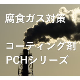
Sulfurization prevention coating agent protects the substrate from corrosive gases!

The ideal coating agent for preventing sulfide! It prevents substrate corrosion with a fluororesin film that has gas barrier properties.

The "PCH Series" is a sulfurization prevention coating agent that protects metals like Ag and Cu from corrosive gases. It not only prevents sulfurization but also protects against moisture, making it ideal for LED mounting substrates. Since this product forms a colorless and transparent film, the total light transmittance does not decrease even after application. To evaluate gas corrosion resistance, we conducted gas corrosion tests to confirm the maintenance rate of gloss before and after testing. The results are detailed with comparative images of the silver plate used as the substrate in its pre-test, uncoated state, and after applying this product. 【Features】 ■ Sulfurization resistance ■ Corrosive gas resistance ■ Moisture and drip protection ■ Adhesion ■ Rust prevention ■ Transparency ■ Room temperature drying

  • Coating Agent
  • LED Module
  • substrate

Added to bookmarks

Bookmarks list

Bookmark has been removed

Bookmarks list

You can't add any more bookmarks

By registering as a member, you can increase the number of bookmarks you can save and organize them with labels.

Free membership registration

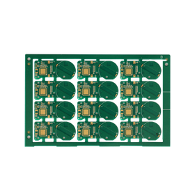
We provide a comprehensive service for the design, manufacturing, and assembly of PCBs and PCBA.

With reliable technical skills and a rich lineup, we can accommodate small lot orders!

H-fast Electronics is a company specialized in the manufacturing of PCBs (printed circuit boards) and PCBAs (printed circuit board assemblies). We have established a production system that allows us to handle everything from raw materials to the manufacturing of bare boards and assembly in-house. This enables us to achieve stable quality control, short delivery times, and cost optimization. 【Strengths of H-fast Electronics】 ✅ Significant reduction in man-hours and delivery times through integrated design, manufacturing, and assembly We provide a comprehensive service for the design, manufacturing, and assembly of PCBs and PCBAs. ✅ Ceramic/Aluminum substrate technology to meet automotive and high heat dissipation needs We cater to a wide range of applications from automotive ceramic/aluminum substrates to general industrial use. ✅ Flexible support from small-scale prototypes to large-scale mass production We accommodate everything from mass production to small lot sizes.

  • 1906281715126708464-002.png
  • 1906281716187620466-002.png
  • 1906281718596594343-002.png
  • Printed Circuit Board
  • Other electronic parts
  • substrate

Added to bookmarks

Bookmarks list

Bookmark has been removed

Bookmarks list

You can't add any more bookmarks

By registering as a member, you can increase the number of bookmarks you can save and organize them with labels.

Free membership registration

[Quality Policy] Trust in the Inspection Process

The entire history from material input to completed shipment is on this one sheet.

Each customer's order will be assigned a production item number, and a process communication document will be issued to record the steps until shipment. After shipment, inquiries and product issues can be addressed at any time using the production item number. ★Assembly Completion Inspection★ All items after assembly will be inspected using an inspection sheet. The standardized work at each stage confirms the quality that has already been integrated into the process. The first lot will be recorded on standard format paper, and from the second lot onward, all records will be handwritten in a modified format of the standard template. This is stored within the factory for a certain period as work history, allowing for immediate reference at any time. ★Storage of Various Records★ Manufacturing records are kept from the history of parts and materials to inspection records. They can be searched and referenced immediately in response to customer inquiries. Records related to printed circuit board assembly, inspection logs, and inspection records of assembly site work are managed internally with unique identifiers, organized by model.

  • Circuit board design and manufacturing
  • substrate

Added to bookmarks

Bookmarks list

Bookmark has been removed

Bookmarks list

You can't add any more bookmarks

By registering as a member, you can increase the number of bookmarks you can save and organize them with labels.

Free membership registration

Quality Policy: Soldering Skill Certification System

Only those who pass will perform soldering work under the 'Skill Certification System.'

[PWB Implementation One Skill Quality Certificate] At Shinjitsu, we have established an internal soldering skill certification system since 2007 to improve the manual soldering techniques that are the foundation of implementation technology. An internal soldering skill certification committee has been formed, and those who have obtained the Advanced Operator Technical Certificate through the Japan Welding Engineering Society's soldering skill certification exam are appointed to train newcomers according to established procedures. ■ Pre-training Course To obtain certification, participants undergo several days of training conducted by qualified instructors from the Japan Welding Engineering Society. After systematically learning about the history of soldering, basic terminology, fundamental knowledge of printed circuit boards and electronic circuit components, and soldering evaluation criteria using textbooks, they receive practical training and take the exam. ■ Practical Exam In the practical exam, five items are comprehensively evaluated, including the degree of tilt of each component, lead forming, cleanliness, and required time. Upon passing, a certificate is awarded, granting the qualification to perform soldering work on customer circuit boards for the first time. *For more details, please refer to the PDF document or feel free to contact us.

  • Circuit board design and manufacturing
  • substrate

Added to bookmarks

Bookmarks list

Bookmark has been removed

Bookmarks list

You can't add any more bookmarks

By registering as a member, you can increase the number of bookmarks you can save and organize them with labels.

Free membership registration

Quality Policy: Information Security Regulations

Information security measures to protect customer information.

At Sōshin, we aim to develop innovative services that meet market demands, contribute to the benefits of our business partners regarding supply, strive to improve their quality, and enhance customer satisfaction. To achieve this goal, we establish information security regulations to protect the confidentiality of important information of our business partners, ensuring that secure business transactions can continue indefinitely. Additionally, management and employees work together to maintain and improve this system. ◆◆ "SECURITY ACTION" ★★ Two Stars Declaration ◆◆ At Sōshin, we have declared "★★ Two Stars" in the "SECURITY ACTION" program established by the Information-technology Promotion Agency (IPA) to engage in more secure information security measures. *For more details, please refer to the PDF document or feel free to contact us.

  • Circuit board design and manufacturing
  • substrate

Added to bookmarks

Bookmarks list

Bookmark has been removed

Bookmarks list

You can't add any more bookmarks

By registering as a member, you can increase the number of bookmarks you can save and organize them with labels.

Free membership registration

Quad Lock LN Bias Board 'LN-SD24-E01'

Ideal for RF modulation applications requiring high S/N! It allows for external monitoring of operating conditions.

The "LN-SD24-E01" is a Quad Lock LN bias board designed for equipment integration. It is compatible with LN modules from various manufacturers, including EOspace, and outputs a maximum DC bias voltage of ±15V. Additionally, since it is designed for equipment integration, it can be used immediately by simply connecting the power supply. The output noise of the DC bias voltage is ultra-low, with less than 3μV/√Hz up to 10kHz and less than 20nV/√Hz above 100kHz, making it suitable for RF modulation applications that require high S/N. 【Features】 ■ Compatible with various LN modules ■ Designed for equipment integration ■ ±15V DC bias output ■ Ultra-low noise ■ Built-in PD *For more details, please refer to the PDF document or feel free to contact us.

  • Other electronic parts
  • substrate

Added to bookmarks

Bookmarks list

Bookmark has been removed

Bookmarks list

You can't add any more bookmarks

By registering as a member, you can increase the number of bookmarks you can save and organize them with labels.

Free membership registration

Printed Circuit Board Business Products and Services

Improved performance in heat dissipation, dust resistance, and water resistance! Ensures the reliability of the mounted circuit board.

At Yoho Electronics, we achieve high product quality and reduced lead times through a consistent production system, unique manufacturing technology, and a quality control framework. The supported substrates include double-sided boards, high multilayer boards, aluminum boards, paper phenolic boards, flexible boards (FPC boards), and ceramic boards. By molding (resin encapsulation) the assembled boards, we enhance performance in heat dissipation, dust resistance, and drip resistance, ensuring the reliability of the assembled boards. In addition to molding, we can also accommodate substrate coating. 【Products and Services】 <Supported Substrates> ■ Double-sided boards, high multilayer boards, aluminum boards, paper phenolic boards, flexible boards (FPC boards), ceramic boards, etc. *For more details, please refer to the PDF document or feel free to contact us.

  • Circuit board design and manufacturing
  • Circuit board processing machine
  • substrate

Added to bookmarks

Bookmarks list

Bookmark has been removed

Bookmarks list

You can't add any more bookmarks

By registering as a member, you can increase the number of bookmarks you can save and organize them with labels.

Free membership registration

Business Introduction of Nitto Corporation

Ultra-precision grinding processing! Introduction to the business of Nitto Corporation.

At Nitto Corporation, we are engaged in the development and manufacturing of flat glass, which is essential for information devices, including LCD (liquid crystal display) glass and glass substrates used in hard disks. We pursue extreme smoothness precision in our polishing processes, boasting a smoothness accuracy of 2 angstroms with our in-house developed equipment and high technical skills. We meet the diverse needs of high-tech industries, including office automation equipment, telecommunications, home appliances, AV, and medical devices. In quality control, we provide reliable products under meticulous and stringent quality inspections within a clean room that maintains a high-level environment with a cleanliness class of 100. **Features** - Extreme smooth polishing processing - Highly reliable quality control - Thorough environmental management system - Monthly processing achievements of over several million pieces - Versatile cutting, chamfering, and centering processing - ISO 9001 certification obtained - ISO 14001 certification obtained For more details, please contact us or download the catalog.

  • Other processing machines
  • substrate

Added to bookmarks

Bookmarks list

Bookmark has been removed

Bookmarks list

You can't add any more bookmarks

By registering as a member, you can increase the number of bookmarks you can save and organize them with labels.

Free membership registration

Ultra-precision grinding processing and achievements

Production record of over several million sheets per month! Achieving an extreme thinness that causes the glass to warp under its own weight, with an ultimate level of flatness.

We would like to introduce our ultra-precision polishing processing and achievements. In fields such as photomasks, LCD panels, and various optical filters, where high precision is required, we have achieved a balance between precision and mass production. What makes this possible is our in-house developed double-sided polishing machine. While maintaining the highest level of processing precision, we have a track record of processing over several million pieces per month. 【Features】 ■ We can also handle processing from material procurement. ■ We do not limit ourselves to specific materials; we work with glass, ceramics, plastics, and metals. ■ We have extensive experience with difficult-to-polish glasses such as colored glass (optical glass) and IR cut glass. ■ We can process LCD panels to a thickness of 0.1mm. *For more details, please refer to the PDF document or feel free to contact us.

  • Processing Contract
  • substrate

Added to bookmarks

Bookmarks list

Bookmark has been removed

Bookmarks list

You can't add any more bookmarks

By registering as a member, you can increase the number of bookmarks you can save and organize them with labels.

Free membership registration

Cable checker

Introducing the cable checker.

Hirose Technical Research Institute's "HIROSE" Cable Checker *For more details, please download the materials or contact us directly. 【Industries Actively Hiring】 ■ Power Industry (Thermal Power Plants, Nuclear Power Plants) ■ Chemical Industry (Chemical Plants, Manufacturing, etc.) ■ Electrical Manufacturing Industry/Field ■ Automotive Industry, Machinery, Heavy Industry

  • relay
  • substrate

Added to bookmarks

Bookmarks list

Bookmark has been removed

Bookmarks list

You can't add any more bookmarks

By registering as a member, you can increase the number of bookmarks you can save and organize them with labels.

Free membership registration

Hanoh Manufacturing Co., Ltd. Business Introduction

We specialize in "high quality and short delivery times" through small quantities of various products and in-house integrated production!

Since our establishment in 1950, we have progressed alongside the history of the development of the electronics industry, engaging in technology development that brings joy to many of our valued customers, and we have achieved steady growth. Moving forward, in the increasingly important field of the electronics industry, we are committed to refining our integrated production system, including our development team, to respond comprehensively to your needs. Additionally, while considering the global environment, we will strive to deliver products that satisfy you in terms of quality, price, and delivery time, with creativity and enthusiasm. We look forward to your continued guidance and encouragement. 【Business Introduction (Partial)】 ■ Development Support ■ Printed Circuit Board Design ■ Printed Circuit Board Manufacturing *For more details, please refer to the PDF document or feel free to contact us.

  • Printed Circuit Board
  • Processing Contract
  • Contract manufacturing
  • substrate

Added to bookmarks

Bookmarks list

Bookmark has been removed

Bookmarks list

You can't add any more bookmarks

By registering as a member, you can increase the number of bookmarks you can save and organize them with labels.

Free membership registration