We have compiled a list of manufacturers, distributors, product information, reference prices, and rankings for substrate.
ipros is IPROS GMS IPROS One of the largest technical database sites in Japan that collects information on.

substrate Product List and Ranking from 577 Manufacturers, Suppliers and Companies | IPROS GMS

Last Updated: Aggregation Period:Jul 29, 2026~Aug 25, 2026
This ranking is based on the number of page views on our site.

substrate Manufacturer, Suppliers and Company Rankings

Last Updated: Aggregation Period:Jul 29, 2026~Aug 25, 2026
This ranking is based on the number of page views on our site.

  1. 共立エレックス Saga//Ceramics
  2. スクリーンプロセス Kanagawa//others
  3. 太洋テクノレックス 本社 和歌山 Wakayama//Electronic Components and Semiconductors
  4. 4 山下マテリアル Kanagawa//Electronic Components and Semiconductors
  5. 5 アイン 本社工場 Nagano//Electronic Components and Semiconductors

substrate Product ranking

Last Updated: Aggregation Period:Jul 29, 2026~Aug 25, 2026
This ranking is based on the number of page views on our site.

  1. Ceramic substrate for firing setters 共立エレックス
  2. <Super Short Delivery Time> Base Material Specification Sheet スクリーンプロセス
  3. PICLIA Ribbon Dual Sensor (Piezoelectric & Capacitive) *Evaluation Kit DAIKIN FINETECH, LTD.
  4. 4 Long-sized printed circuit board ☆ up to 1500mm ☆ Ally Japan 横浜本社
  5. 5 Tokyo Machine and Tool Co., Ltd. Business Introduction 東京マシン・アンド・ツール

substrate Product List

1681~1710 item / All 1972 items

Displayed results

Short delivery time, high quality, low price! Printed circuit board prototyping service *Documentation available

[Materials Available] We will solve your problems! Introduction of printed circuit board prototyping service examples!

"Sarolution" specializes in prototype printed circuit boards, characterized by "short delivery times," "high quality," and "low prices." By limiting the specifications of the circuit boards, we have achieved a low-cost service. We have also established a short delivery service system required for development prototypes. All data checks are conducted in-house, and we generally accept the boards, perform random checks, and then ship them. We also ensure a comprehensive support system after delivery. 【Must-read for those with the following concerns】 - I have an interesting product idea, but my budget is limited... - I need to create a prototype quickly to bring it to market... - I want to try using overseas circuit boards, but I don't have any connections... - Domestic prototype circuit board services have various restrictions... 【Features of Sarolution】 - We can accommodate even one board. Delivery times as short as 2 days! - No initial costs! Shipping included! - You can choose the specifications! - Supports various data formats! Panel editing is also available! *For more details, please download the PDF or feel free to contact us.

  • Printed Circuit Board
  • substrate

Added to bookmarks

Bookmarks list

Bookmark has been removed

Bookmarks list

You can't add any more bookmarks

By registering as a member, you can increase the number of bookmarks you can save and organize them with labels.

Free membership registration

AD7172CM(4)

It is a 24-bit AD converter board.

This is a 24-bit AD converter board using a super low noise AD converter IC. It connects to a computer via USB. There are 4 input channels, and the input voltage range is 0V to +5V. The analog input circuit and the USB connection circuit are isolated.

  • Other measurement, recording and measuring instruments
  • substrate

Added to bookmarks

Bookmarks list

Bookmark has been removed

Bookmarks list

You can't add any more bookmarks

By registering as a member, you can increase the number of bookmarks you can save and organize them with labels.

Free membership registration

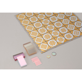
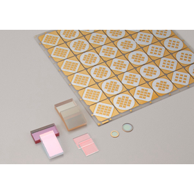
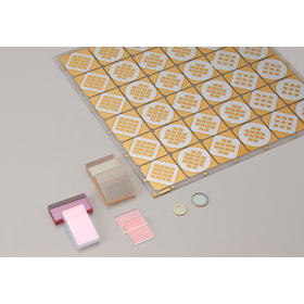
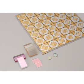
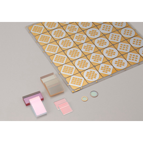
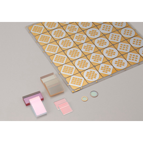
Quartz substrate for semiconductor lithography

End face grinding, bevel grinding, and other round polishing support! Compatible with 6 inches.

In the semiconductor lithography industry, high-precision pattern transfer is required. In particular, the quality of quartz substrates during the exposure process significantly affects device performance. Distortion and surface unevenness of the substrates can reduce pattern accuracy and lead to lower yields. Our quartz substrates are compatible with notch processing and olifura processing, and can also accommodate edge polishing and bevel polishing, enabling high-precision lithography processes. 【Usage Scenarios】 - Mask substrates in the lithography process - Wafer manufacturing processes - Various optical components 【Benefits of Implementation】 - Achievement of high-precision pattern transfer - Contribution to yield improvement - Adaptability to diverse processing needs

  • Processing Contract
  • substrate

Added to bookmarks

Bookmarks list

Bookmark has been removed

Bookmarks list

You can't add any more bookmarks

By registering as a member, you can increase the number of bookmarks you can save and organize them with labels.

Free membership registration

Quartz substrate for optical lenses

Perfect for lens processing! Leave the precision machining of quartz substrates to us.

In the optical lens industry, high transmittance and precise shapes are required. The performance of the lens is greatly influenced by the quality of the substrate, and even slight distortions or surface roughness can degrade optical performance. Our quartz substrates can be processed to meet customer needs, including notch processing and olifura processing. 【Usage Scenarios】 - Optical lenses - Various filters - Prisms 【Benefits of Implementation】 - Enables high-precision lens processing - Improves optical characteristics - Accommodates diverse shapes

  • Processing Contract
  • substrate

Added to bookmarks

Bookmarks list

Bookmark has been removed

Bookmarks list

You can't add any more bookmarks

By registering as a member, you can increase the number of bookmarks you can save and organize them with labels.

Free membership registration

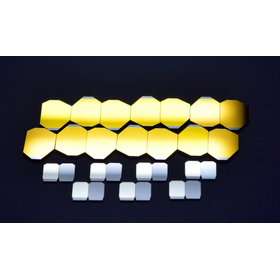
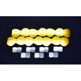
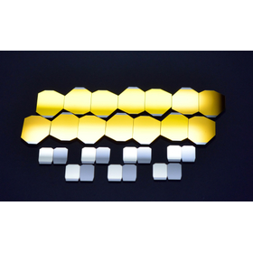
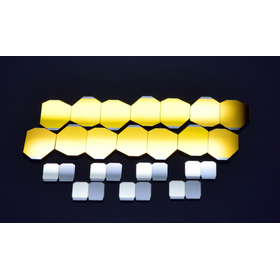
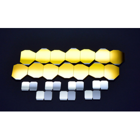
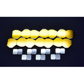
Quartz substrate for lasers

Ideal for laser mirrors! Achieving high-precision optical performance through precision processing.

In the laser industry, high-quality mirror substrates are required to optimize the reflection and transmission characteristics of laser light. Particularly in high-power lasers and precision optical systems, the accuracy of the substrate significantly affects the performance of the laser. Distortion and surface roughness of the substrate can lead to attenuation of the laser light and a decrease in beam quality. Our quartz substrates can be processed to meet customer needs, including edge polishing and bevel polishing. They achieve high optical characteristics and durability, contributing to the performance enhancement of laser systems. 【Application Scenes】 - Laser oscillators - Laser processing machines - Optical experiments 【Effects of Implementation】 - Improvement of laser light reflectivity and transmittance - Enhancement of beam quality - Increased stability of laser systems

  • Processing Contract
  • substrate

Added to bookmarks

Bookmarks list

Bookmark has been removed

Bookmarks list

You can't add any more bookmarks

By registering as a member, you can increase the number of bookmarks you can save and organize them with labels.

Free membership registration

Quartz substrate for research institutions

Perfect for experimental purposes! Leave the precision processing of quartz substrates to us.

In experiments conducted at research institutions, high-precision quartz substrates are required. Particularly in optical experiments and precision measurements, the quality of the substrate significantly affects the experimental results. We accommodate various processing methods such as edge polishing and bevel polishing to meet the needs of experiments. Our products can be customized to customer specifications, including notch processing and olifura processing. 【Usage Scenarios】 - Optical experiments - Precision measurements - Various experimental substrates 【Benefits of Implementation】 - Improved experimental accuracy - Adaptation to diverse experiments - Provision of high-quality substrates

  • Processing Contract
  • substrate

Added to bookmarks

Bookmarks list

Bookmark has been removed

Bookmarks list

You can't add any more bookmarks

By registering as a member, you can increase the number of bookmarks you can save and organize them with labels.

Free membership registration

Glass substrate

We manufacture various glass substrates such as soda glass, borosilicate glass, and quartz.

We will manufacture items in your desired size using materials such as soda glass, Eagle XG, Tempax, B270 (whiteboard), and quartz.

  • Glassware and containers
  • substrate

Added to bookmarks

Bookmarks list

Bookmark has been removed

Bookmarks list

You can't add any more bookmarks

By registering as a member, you can increase the number of bookmarks you can save and organize them with labels.

Free membership registration

Glass capillary tube

We manufacture glass capillaries in various sizes.

We have inexpensive BC glass capillaries (grade 2 hard glass) and Pyrex equivalent (grade 1 hard glass) capillaries that can accommodate your desired outer and inner diameters. - For experimental and research equipment. - As parts for machinery, etc. They are being used.

  • Glassware and containers
  • substrate

Added to bookmarks

Bookmarks list

Bookmark has been removed

Bookmarks list

You can't add any more bookmarks

By registering as a member, you can increase the number of bookmarks you can save and organize them with labels.

Free membership registration

Densitron QVGA LCD LED backlight power supply board

This is the original LED backlight power supply board from Kenic System.

The "KSLBC-3(D2)" is an LED backlight power supply board for QVGA LCDs manufactured by Densitron. 【Features】 - It can be easily configured with a general-purpose microcontroller for ON/OFF and brightness adjustment. - It uses a device with built-in overvoltage protection, so even if the LED is disconnected, the device is protected. - It is compact and lightweight, measuring 67×20mm.

  • controller
  • substrate

Added to bookmarks

Bookmarks list

Bookmark has been removed

Bookmarks list

You can't add any more bookmarks

By registering as a member, you can increase the number of bookmarks you can save and organize them with labels.

Free membership registration

Low-damage processing and polishing processes and evaluation of SiC and GaN wafer substrates.

Latest polishing technology for various GaN/SiC related materials with high hardness and brittleness.

★What does the future hold for technologies that support large-diameter processing and mass production techniques? ★We will also introduce the characteristics of the residual processing altered layer remaining during SiC wafer processing, its impact on subsequent processes, and analysis techniques for the altered layer. ★We are currently conducting a pre-content request service! We welcome your practical challenges! 【Venue】 Tekno Kawasaki, 5th Floor, 5th Training Room【Kanagawa, Kawasaki】 【Date and Time】 September 17, 2013 (Tuesday) 11:00-15:45 【Instructors】 Part 1: Dr. Tomohisa Kato, Team Leader and Senior Researcher, Advanced Power Electronics Research Center, National Institute of Advanced Industrial Science and Technology (AIST) Here is the homepage of the Advanced Power Electronics Research Center. Part 2: Representative from Namiki Precision Jewel Co., Ltd., NJC Technology Research Institute Part 3: Professor Kazuto Yamauchi, Graduate School of Engineering, Osaka University

  • Company:AndTech
  • Price:10,000 yen-100,000 yen
  • Technical Seminar
  • substrate

Added to bookmarks

Bookmarks list

Bookmark has been removed

Bookmarks list

You can't add any more bookmarks

By registering as a member, you can increase the number of bookmarks you can save and organize them with labels.

Free membership registration

[Information] President's Blog December 2020

It provides a detailed explanation of "What is a Smith chart?" using diagrams and photos!

This document summarizes the president's blog of Wave Technology Co., Ltd., a "development design promotion business" that addresses the shortage of engineers, from December 4, 2020, to December 17, 2020. Starting with the announcement of the exhibition participation on December 4, 2020, "Following up on the previous announcement of our exhibition," and introducing "What is a Smith chart?" on December 8, 2020. In addition, we have published a wealth of useful information related to products and industries. Please take a moment to read it. [Contents] ■ December 4, 2020: Following up on the previous announcement of our exhibition participation. ~ Virtual Exhibition HYOGO! ~ ■ December 8, 2020: What is a Smith chart? ~ Let's visualize the Smith chart ~ ■ December 17, 2020: It's not just for engineers. Sales training can also be rapidly learned with Tech Sherpa. *For more details, please refer to the PDF document or feel free to contact us.

  • Other contract services
  • Embedded system design service
  • Circuit board design and manufacturing
  • substrate

Added to bookmarks

Bookmarks list

Bookmark has been removed

Bookmarks list

You can't add any more bookmarks

By registering as a member, you can increase the number of bookmarks you can save and organize them with labels.

Free membership registration

[Data] Shirutoku Report No. 10 #Metal Enclosure

How is a metal casing made? A brief introduction to processing methods and design techniques.

★★Shirutoku Report: Useful Information You Can Benefit From★★ Without further ado, I will talk about the metal enclosures I am currently involved in developing. There are various processing methods for creating metal enclosures, and the design approach changes depending on the processing method. This report briefly introduces the representative processing methods and design approaches for metal enclosures. [Contents] ■ Press bending processing ■ Deep drawing processing ■ Die casting *For more details, please refer to the PDF document or feel free to contact us.

  • Mold Design
  • Processing Contract
  • substrate

Added to bookmarks

Bookmarks list

Bookmark has been removed

Bookmarks list

You can't add any more bookmarks

By registering as a member, you can increase the number of bookmarks you can save and organize them with labels.

Free membership registration

[Information] Shirutoku Report No. 20 #Tips for Reducing PCB Costs

It is also possible to reduce high manufacturing initial costs! Here are some tips for reducing the cost of printed circuit boards.

★★Shirutoku Report: Useful Information You Should Know★★ Printed circuit boards (PCBs) are relatively expensive components among electronic devices, and depending on the quality of the design, the use of the board may change, which can impact costs. You might consider searching for inexpensive PCB manufacturers overseas and adopting them, but the factors that significantly affect the cost of printed circuit boards are "board structure/layer count" and "board size." This report focuses on "board size" and introduces tips for reducing PCB costs. [Contents] ■ Tips for Reducing Costs Based on Board Size *For more details, please refer to the PDF document or feel free to contact us.*

  • Printed Circuit Board
  • substrate

Added to bookmarks

Bookmarks list

Bookmark has been removed

Bookmarks list

You can't add any more bookmarks

By registering as a member, you can increase the number of bookmarks you can save and organize them with labels.

Free membership registration

[Information] Shirutoku Report No. 95 # Effective Components for Noise Countermeasures

I will talk about the noise countermeasures in the evaluation of power converters!

★★Shirutoku Report: Useful Information You Can Benefit From★★ The current task is the evaluation of "power conditioners" (hereinafter referred to as power conditioners). When we talk about "evaluation of power conditioners," there are various types of evaluations, but this time I would like to discuss the noise countermeasures implemented in our recent work. Please take a moment to read it. [Contents] ■ Causes of Noise Generation ■ Noise Countermeasure Component "Core (Core Material of the Coil)" *For more details, please refer to the PDF document or feel free to contact us.

  • Other electronic parts
  • substrate

Added to bookmarks

Bookmarks list

Bookmark has been removed

Bookmarks list

You can't add any more bookmarks

By registering as a member, you can increase the number of bookmarks you can save and organize them with labels.

Free membership registration

Transparent substrate "SPET"

Due to its reflow heat resistance of 180°C and high-temperature storage resistance of 120°C, it is suitable for soldering electronic components.

"SPET" is a highly heat-resistant and low-resistance transparent substrate that, despite being PET, enhances LED driving, increases the sensitivity of electrostatic switches, and improves antenna characteristics. The total light transmittance of the substrate is 90.0%, with a haze of 0.8, and it features fine wiring that is difficult to see. Additionally, the sheet resistance of the conductor is 0.95 mΩ/□, and the conductor thickness is 18 μm, making it suitable for use as a substrate. [Features] ■ High transparency substrate ■ Low resistance conductor ■ High heat-resistant substrate *For more details, please refer to the related links or feel free to contact us.

  • Printed Circuit Board
  • substrate

Added to bookmarks

Bookmarks list

Bookmark has been removed

Bookmarks list

You can't add any more bookmarks

By registering as a member, you can increase the number of bookmarks you can save and organize them with labels.

Free membership registration

What is SPET?

Tightly laminated resist, copper foil, adhesive layer, and PET! Introducing our transparent substrate.

"SPET" is a single-sided substrate made by laminating copper foil onto a PET base material. The base material thickness is 100μm/188μm, and the copper foil thickness is 12μm/18μm. It is a product that is tightly laminated with resist, copper foil, adhesive layer, and PET. Additionally, we also offer "SPET-MM," which has wiring that is nearly invisible. Please feel free to contact us when you need assistance. 【Features】 ■ High transparency flexible substrate ■ Low-resistance conductor due to copper foil lamination ■ Compatible with low-temperature soldering (180°C) *For more details, please refer to the related links or feel free to contact us.

  • Printed Circuit Board
  • substrate

Added to bookmarks

Bookmarks list

Bookmark has been removed

Bookmarks list

You can't add any more bookmarks

By registering as a member, you can increase the number of bookmarks you can save and organize them with labels.

Free membership registration

[Introduction to the Fair Process] Manufacturing/Assembly/Inspection/Packaging

The product, along with the instruction manual, is placed in a dedicated individual box and shipped directly to the customer's specified factory! Electrical testing can also be performed.

At Fair Co., Ltd., we perform harness processing, sheet metal assembly, and circuit board installation, among other tasks. We can also program and conduct electrical inspections, and in cases of high production volume, we create dedicated jigs to enhance production efficiency. Additionally, we handle projects that involve placing instruction manuals in dedicated packaging boxes along with the products and shipping them directly to the customer's specified factory. 【Other Process Examples (Excerpt)】 ■ Product Planning ■ CPU Firmware Design ■ Circuit Board Pattern Design ■ Component Procurement ■ Component Mounting *For more details, please refer to the related links or feel free to contact us.

  • Other contract services
  • substrate

Added to bookmarks

Bookmarks list

Bookmark has been removed

Bookmarks list

You can't add any more bookmarks

By registering as a member, you can increase the number of bookmarks you can save and organize them with labels.

Free membership registration

Circuit board design achievements

We undertake design work in various fields, including precision machinery, industrial equipment, and medical devices!

We would like to introduce our achievements in "circuit board design." We support various genres of design, including precision and industrial equipment such as BMS devices for storage batteries and car-sharing related equipment, as well as medical devices, agricultural equipment, and consumer electronics. Please feel free to contact us when you need our services. 【Circuit Board Design Achievements (Partial)】 ■ Precision and Industrial Equipment - BMS devices for storage batteries - Car-sharing related equipment - Non-destructive device scintillator (for baggage inspection/electronic component internal inspection) - Wind turbine component monitoring devices - Wireless communication devices *For more details, please refer to our company brochure.

  • Circuit board design and manufacturing
  • substrate

Added to bookmarks

Bookmarks list

Bookmark has been removed

Bookmarks list

You can't add any more bookmarks

By registering as a member, you can increase the number of bookmarks you can save and organize them with labels.

Free membership registration

Printed circuit board design high-frequency board

We accept artwork design for various types of boards, including high-frequency impedance control boards and power supply boards.

We specialize in the design of impedance control PCBs, with proven experience in high-frequency boards ranging from 10GHz to 40GHz and high-speed transmission boards from 40Gbps to 100Gbps. Additionally, we consider various aspects from PCB manufacturing to component mounting and propose the optimal layout.

  • others
  • substrate

Added to bookmarks

Bookmarks list

Bookmark has been removed

Bookmarks list

You can't add any more bookmarks

By registering as a member, you can increase the number of bookmarks you can save and organize them with labels.

Free membership registration

Rigid flex circuit impedance

We also accept prototyping and small lot production of rigid-flex PCBs from AW design at our array.

By combining rigid substrates with bendable flexible substrates, various layouts become possible.

  • Prototype Services
  • others
  • substrate

Added to bookmarks

Bookmarks list

Bookmark has been removed

Bookmarks list

You can't add any more bookmarks

By registering as a member, you can increase the number of bookmarks you can save and organize them with labels.

Free membership registration

Flexible printed circuit board (FPC) impedance control

Impedance control of flexible substrates and UL certification can be achieved with short lead times and small lot production.

We can respond to circuit board manufacturing and component assembly in just one working day at the shortest. Additionally, we manufacture high-performance flexible circuit boards with impedance control during the artwork design phase. We can also accommodate small lot production. Please feel free to consult with us.

  • others
  • Prototype Services
  • substrate

Added to bookmarks

Bookmarks list

Bookmark has been removed

Bookmarks list

You can't add any more bookmarks

By registering as a member, you can increase the number of bookmarks you can save and organize them with labels.

Free membership registration

Flexible printed circuit board (FPC) [Solving the issues in the prototype development of flexible printed circuit boards!]

Solving the issues of prototype development for flexible PCBs with many limitations! We manufacture high-performance flexible PCBs!

We can respond to circuit board manufacturing and component mounting in as little as one working day each. Additionally, we manufacture high-performance flexible circuit boards with impedance control during artwork design. We also accommodate small lot production. 【We can also support the following specifications】 ■ Component mounting FPC (double-sided mounting, lead-free mounting, mounter/reflow, bare chip mounting) ■ Bonding processing with other boards using ACF (FPC + FPC, FPC + PBC, FPC + glass substrate, etc.) ■ Multi-layer FPC (supports 3 to 6 layers; double-sided mounting is also possible) ■ Fine pitch FPC (single-sided board... minimum L/S 12/30μm; double-sided board... minimum L/S 25/50μm) *For details, please request materials or view the PDF data from the download.

  • others
  • substrate

Added to bookmarks

Bookmarks list

Bookmark has been removed

Bookmarks list

You can't add any more bookmarks

By registering as a member, you can increase the number of bookmarks you can save and organize them with labels.

Free membership registration

Tokaishin'e Electronics Industry Multi-layer Circuit Board

We have a variety of products available to meet the diverse needs of our customers.

It is a substrate with copper foil on both sides and inside of a glass epoxy insulating board.

  • Other services
  • substrate

Added to bookmarks

Bookmarks list

Bookmark has been removed

Bookmarks list

You can't add any more bookmarks

By registering as a member, you can increase the number of bookmarks you can save and organize them with labels.

Free membership registration

Daichang Electronics Flex-Rigid Circuit Boards

We aim to be a company where everyone can thrive and enjoy their work.

The business environment surrounding our company has become characterized by significant changes akin to turbulence. In order to achieve sustainable development without being swayed by economic trends, we will take the initiative to lead change and proactively embrace challenges.

  • Other network tools
  • substrate

Added to bookmarks

Bookmarks list

Bookmark has been removed

Bookmarks list

You can't add any more bookmarks

By registering as a member, you can increase the number of bookmarks you can save and organize them with labels.

Free membership registration

Daichang Electronics Build-Up Multilayer Circuit Board

We aim to be a company where everyone can thrive and enjoy their work.

The business environment surrounding our company has become characterized by significant changes akin to turbulence. In order to achieve sustainable development without being swayed by economic trends, we will take the initiative to lead change and proactively embrace challenges.

  • Other network tools
  • substrate

Added to bookmarks

Bookmarks list

Bookmark has been removed

Bookmarks list

You can't add any more bookmarks

By registering as a member, you can increase the number of bookmarks you can save and organize them with labels.

Free membership registration

Small lot for development! For automotive and power supply use. Thick copper substrate (high current substrate).

With a maximum copper thickness of 400μm, it is suitable for heat dissipation measures and power supply for power devices! It can also be formed on substrates such as transformers and motors.

Meito Electric's "Thick Copper Substrate (High Current Substrate)" is suitable for heat dissipation and current supply in heating devices used in automotive and power supply applications. By increasing the conductor (copper) thickness compared to the conventional 35μm, power circuits and control circuits can be formed on the same substrate. The creation of thick copper coil patterns allows for the construction of transformer circuits and motor circuits on the substrate. 【Substrate Specifications】 ■ Outer layer copper foil thickness: 70μm to 200μm ■ Inner layer copper foil thickness: 70μm to 400μm ■ High thermal conductivity resin: up to 8W/mK ■ Bonding: High thermal conductivity resin and copper, etc. ■ Number of layers: Proven from 2 layers to 10 layers (specifications to be discussed) ■ Copper plate: C1020 (oxygen-free) or C1100 (tough pitch) *For detailed information, please download the PDF or feel free to contact us.

  • Contract manufacturing
  • substrate

Added to bookmarks

Bookmarks list

Bookmark has been removed

Bookmarks list

You can't add any more bookmarks

By registering as a member, you can increase the number of bookmarks you can save and organize them with labels.

Free membership registration