See Semiconductor Manufacturing Equipment's detailed category ranking
- CVD Equipment
- Sputtering Equipment
- Annealing furnace
- Coater
- Resist Device
- Oxidation/Diffusion Device
- Stepper
- Etching Equipment
- Ion implantation equipment
- Ashing device
- Evaporation Equipment
- Electron beam lithography equipment
- Tester
- Semiconductor inspection/test equipment
- Wafer processing/polishing equipment
- Molding Equipment
- Bonding Equipment
- CMP Equipment
- Photomask
- Other semiconductor manufacturing equipment

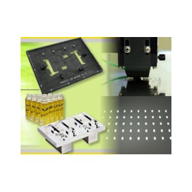
A sheet socket that enables stable inspection in semiconductor back-end process inspection! What is "PCR" that allows for high-speed and high-density measurements? Technical materials on operating principles and more will be provided!

If you have challenges with streamlining wet processes or saving space, this is a must-see. We are currently offering materials that introduce an overview of process integration technology.

Numerous adoption results worldwide. We propose suitable solutions for automatic plating solution analysis in various electroplating and electroless plating processes, as well as in the Cu damascene process.

Visualize surface foreign substances, dirt, and scratches! It is well-received as a daily management tool for yield management, quality control, cleaning management, and hygiene management. *Demo units available for loan.

A clear explanation of case studies related to semiconductor testing, divided into four sections: background, issues, implementation, and results!

MOCVD, filter, AIXTRON, LED, made in China, high-temperature vacuum dust filtration.

Far superior in corrosion resistance and plasma resistance compared to protective films created by thermal spraying or aerosol deposition! Yttrium oxide produced by a unique ion-assisted deposition method.
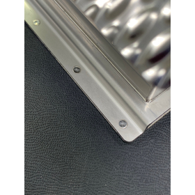
Goodbye, dents. By replacing spot welding with fiber laser welding, it is possible to achieve such beautiful welds that finishing of dents is unnecessary!

Ideal for testing resin and plastic raw materials! Our uniquely developed inspection mechanism detects foreign substances and discoloration in pellets and powders! *Detection of 9μm is possible.

We can repair over 150 semiconductor manufacturing equipment manufacturers! We offer flexible responses regarding delivery times and quality assurance.

We manufacture small, low-cost, and quick-delivery equipment suitable for research, prototype production, die, gravure, roll coat, and roll-to-roll applications! *Test coating services are also available!


