substrateのメーカーや取扱い企業、製品情報、参考価格、ランキングをまとめています。
イプロスは、 製造業 ・ BtoB における情報を集めた国内最大級の技術データベースサイトです。

substrate - メーカー・企業580社の業務用製品ランキング | イプロスものづくり

更新日: 集計期間:Sep 09, 2026~Oct 06, 2026
※当サイトの各ページの閲覧回数を元に算出したランキングです。

substrateのメーカー・企業ランキング

更新日: 集計期間:Sep 09, 2026~Oct 06, 2026
※当サイトの各ページの閲覧回数を元に算出したランキングです。

  1. 山下マテリアル Kanagawa//Electronic Components and Semiconductors
  2. スクリーンプロセス Kanagawa//others
  3. ユメックス Saitama//Electronic Components and Semiconductors
  4. 4 沖電気工業 産業営業本部 産業営業統括室 Tokyo//Information and Communications
  5. 5 プリケン 本社、山形営業所、神奈川営業所、関西営業所、福岡営業所 Saitama//Electronic Components and Semiconductors

substrateの製品ランキング

更新日: 集計期間:Sep 09, 2026~Oct 06, 2026
※当サイトの各ページの閲覧回数を元に算出したランキングです。

  1. <Super Short Delivery Time> Base Material Specification Sheet スクリーンプロセス
  2. Electronic equipment development and production ユメックス
  3. PICLIA Ribbon Dual Sensor (Piezoelectric & Capacitive) *Evaluation Kit DAIKIN FINETECH, LTD.
  4. 4 Long-sized printed circuit board ☆ up to 1500mm ☆ Ally Japan 横浜本社
  5. 5 Difficult-to-weld areas! Even when you're out and about! | High-strength adhesive for metals スリーエム ジャパン

substrateの製品一覧

1201~1230 件を表示 / 全 1960 件

表示件数

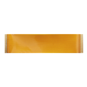
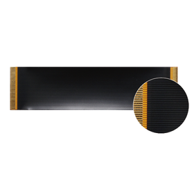
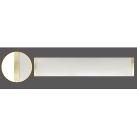
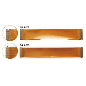
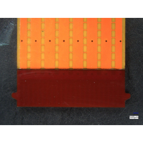
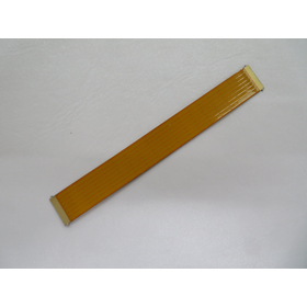
It's also okay to use it twisted! "Flexible substrate compatible with high-speed transmission connectors."

Supports high-speed transmission up to 15GHz! We have combined the high-speed transmission connectors from Irisoh Electronics with our flexible substrates.

The "Flexible substrate compatible with high-speed transmission connectors" combines the high-speed transmission connectors from Irisoh Electronics, [IMSA-11600S-30Y900 and IMSA-11501S-30Y900], with our YFC series (LVDS type microstrip line) RFM. By integrating them, it supports high-speed transmission up to 15GHz. 【Features】 ■ The LVDS-compatible FPC has been slotted. ■ It is easy to bend and can also be twisted for use. *For more details, please refer to the PDF document or feel free to contact us.

ブックマークに追加いたしました

ブックマーク一覧

ブックマークを削除いたしました

ブックマーク一覧

これ以上ブックマークできません

会員登録すると、ブックマークできる件数が増えて、ラベルをつけて整理することもできます

無料会員登録

High Heat Resistance Heat Dissipation Flexible Circuit Board (FPC) *Compatible with 150°C environments

It can suppress discoloration during heating. Here are the test results using a double-sided panel.

The "High Heat Resistant Radiation Flexible Printed Circuit Board (FPC)" is an FPC that uses Okitsumo's heat-resistant solder resist "TAINEX." TAINEX is suitable for high-temperature environments up to 150°C and suppresses discoloration during heating. It also achieves radiation heat dissipation, and in our heat dissipation experiments, when combined with a thermal conduction layer, it has been shown to maintain temperatures more than 30 degrees lower compared to typical resist specifications for FPCs. *This result is based on tests conducted on double-sided boards. 【Features】 ■ FPC using Okitsumo's heat-resistant solder resist "TAINEX" ■ Thermal measures: Achieves a radiation rate of over 90% *For more details, please refer to the PDF document or feel free to contact us.

ブックマークに追加いたしました

ブックマーク一覧

ブックマークを削除いたしました

ブックマーク一覧

これ以上ブックマークできません

会員登録すると、ブックマークできる件数が増えて、ラベルをつけて整理することもできます

無料会員登録

Achieving a thickness of 0.98mm with 12 layers! 'High-Density High-Multilayer Flexible Circuit Board'

When you want to implement high-density wiring with over 200 pins in a limited space! It can be bent for use, allowing for high-density wiring in a compact space.

The "High-Density High-Multilayer Flexible Circuit Board" is an FPC developed for devices that require many signals. Despite having a 12-layer structure, it achieves a thickness of less than 1mm. The cable section can be bent for use, enabling high-density wiring in compact spaces. 【Features】 ■ The harness section can be bent for use. ■ Ideal for applying high-density wiring with over 200 pins in limited spaces. *For more details, please refer to the PDF document or feel free to contact us.

ブックマークに追加いたしました

ブックマーク一覧

ブックマークを削除いたしました

ブックマーク一覧

これ以上ブックマークできません

会員登録すると、ブックマークできる件数が増えて、ラベルをつけて整理することもできます

無料会員登録

Specification for filling holes! "Ultra-small diameter through hole."

It is possible to form through holes with a diameter of 25μm or less on double-sided FPC. Additionally, it is also possible to form holes with a minimum diameter of 20μm and a minimum pad diameter of 95μm.

"Ultra-small diameter through holes" are formed with a diameter of φ20μm on both sides of the FPC through laser processing. It is possible to create holes with a minimum diameter of 20μm and a minimum pad diameter of 95μm. By using through-hole plating to fill the holes and arranging the through holes on the pattern, it enables narrower pitch and contributes to the miniaturization of the product. 【Features】 ■ Formation of through holes with a diameter of Φ25μm or less on both sides of the FPC is possible. ■ The holes are filled with 15μm through-hole plating specifications. *For more details, please refer to the PDF document or feel free to contact us.

ブックマークに追加いたしました

ブックマーク一覧

ブックマークを削除いたしました

ブックマーク一覧

これ以上ブックマークできません

会員登録すると、ブックマークできる件数が増えて、ラベルをつけて整理することもできます

無料会員登録

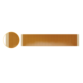
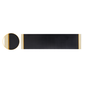
Slit flexible substrate" *can also accommodate "twisting" and "torsion.

Widely used as alternatives for fine coaxial cables, wire harnesses, and cables for medical devices. The spacing and width of the slits can be specified!

The "slit flexible substrate" is a flexible substrate with excellent bendability that has been processed with slits, allowing for "twisting" and "torquing." It is widely used as an alternative to fine coaxial cables, wire harnesses, and cables for medical devices, and since the spacing and width of the slits can be specified, it offers greater freedom for customers. 【Features】 ■ A bendable cable flexible substrate with 0mm slits processed between patterns ■ Can be used with "twisting" and "torquing" compared to conventional products ■ The spacing and width of the slits can be specified *For more details, please refer to the PDF materials or feel free to contact us.

ブックマークに追加いたしました

ブックマーク一覧

ブックマークを削除いたしました

ブックマーク一覧

これ以上ブックマークできません

会員登録すると、ブックマークできる件数が増えて、ラベルをつけて整理することもできます

無料会員登録

Metal-based heat dissipation substrate with low thermal expansion coefficient

For the electrical wiring in the engine room and the gasoline tank meter! Compared to glass epoxy substrates, it has a lower coefficient of thermal expansion and stronger resistance to heat.

The "metal-based heat dissipation substrate" is a substrate that improves heat dissipation through thermal conduction, alleviating thermal issues. There are applications in high-brightness LED lighting (for vehicles and floodlights), as well as in automotive electrical components, ECUs, EPS, and DC/DC converters. Compared to standard glass epoxy substrates, it has a lower thermal expansion coefficient and greater resistance to heat. 【Features】 ■ A substrate that improves heat dissipation through thermal conduction by using metal as the base ■ Compared to standard glass epoxy substrates, it has a lower thermal expansion coefficient and greater resistance to heat *For more details, please refer to the PDF materials or feel free to contact us.

ブックマークに追加いたしました

ブックマーク一覧

ブックマークを削除いたしました

ブックマーク一覧

これ以上ブックマークできません

会員登録すると、ブックマークできる件数が増えて、ラベルをつけて整理することもできます

無料会員登録

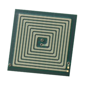
Yamashita Material Flexible Substrate Product Lineup

We have a wide variety of products available, including "high-temperature resistant and oil-resistant FPC" and "high-speed transmission connector compatible FPC"! A new catalog featuring high-current FPC (with signal lines) has also been added.

We would like to introduce the flexible substrates handled by Yamashita Material Co., Ltd. We offer a wide range of products, including the "YFC Normal Type," which can be created in specified lengths, core counts, and pitches, as well as the "High-Temperature Durable and Oil-Resistant FPC," which uses liquid crystal polymer (LCP) for the base and cover materials and has long-term heat resistance of 240°C. Detailed product features, examples of product configurations, and standard specifications are available in our catalog, so please download it for more information. 【Product Lineup (Partial)】 ■ YFC Normal Type ■ YFC Shielded Type ■ YFC Ear Type / Notched Type ■ YFC LVDS Type ■ High-Temperature Durable and Oil-Resistant FPC ■ Long-Term High-Temperature Durable FPC ■ High-Speed Transmission Connector Compatible FPC ■ High-Speed Transmission Multi-Layer FPC ■ High-Density High-Multi-Layer FPC ■ High-Heat-Resistant Heat Dissipation FPC ■ Multi-Layer Coil FPC ■ High-Current FPC with Signal Lines *For more details, please refer to the PDF document or feel free to contact us.

  • スクリーンショット 2021-06-16 133458.png
  • スクリーンショット 2021-06-16 133526.png
  • スクリーンショット 2021-06-16 133555.png
  • スクリーンショット 2021-06-16 133618.png
  • スクリーンショット 2021-06-16 133641.png
  • スクリーンショット 2021-06-16 133840.png
  • スクリーンショット 2021-06-16 134128.png
  • スクリーンショット 2021-06-16 134207.png
  • スクリーンショット 2021-06-16 134229.png
  • Board to FPC connector
  • substrate

ブックマークに追加いたしました

ブックマーク一覧

ブックマークを削除いたしました

ブックマーク一覧

これ以上ブックマークできません

会員登録すると、ブックマークできる件数が増えて、ラベルをつけて整理することもできます

無料会員登録

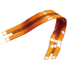
Standard specification product 'BigElec (high current FPC)' for connection between terminal screws.

Suitable for incorporation into curved and narrow spaces. It can form high current circuits with a thin shape and low inductance.

BigElec is a flexible printed circuit board designed for high current wiring, intended as an alternative to busbars and wire harnesses, featuring a slim and flat design. Similar to printed circuit boards, it can accommodate pattern formation and assembly according to your requirements. We have newly introduced the "BigElec Standard Specification Products," which are easy to implement for connections between screw terminals. The BigElec Standard Specification Products have no initial costs, allowing for reduced upfront expenses. 【BigElec Standard Specification Product Specifications】 ■ Layers: 2 layers, 4 layers, 6 layers, 8 layers ■ Wiring width: 8mm to 11mm (integers only) ■ Total length: 30mm to 210mm (integers only) ■ Terminal screw diameters: M3 (hole diameter φ3.8mm), M4 (hole diameter φ4.4mm), M5 (hole diameter φ5.4mm), M6 (hole diameter φ6.5mm), M8 (hole diameter φ8.5mm) *For more details, please download the PDF or contact us.

ブックマークに追加いたしました

ブックマーク一覧

ブックマークを削除いたしました

ブックマーク一覧

これ以上ブックマークできません

会員登録すると、ブックマークできる件数が増えて、ラベルをつけて整理することもできます

無料会員登録

[In Development] GND Slit Structure Flexible Circuit Board

The "GND slit structure technology" solves the issues of "dielectric thickness" and "transmission loss" that arise in microstrip line structures.

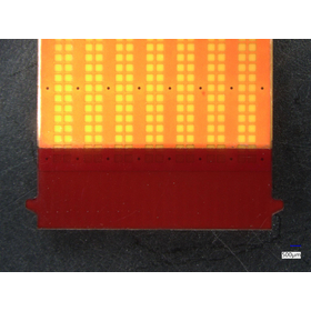
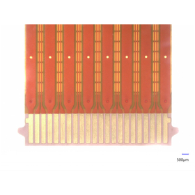
The "GND slit structure" under development addresses the challenges of "dielectric thickness" and "transmission loss" that arise in microstrip line structures. This technology allows for the reduction of dielectric thickness while maintaining transmission characteristics by incorporating a slit design in the GND plane directly beneath the RF line. As a result, it minimizes signal loss while maximizing flexibility. For high-speed transmission compatible YFC products (RFM, RFS series), we provide cable FPCs that reduce transmission loss by adopting the GND slit design, enabling low-loss signal transmission. Please refer to the PDF catalog for the measurement results of transmission loss and flexibility.

  • GNDスリット1.jpg
  • GNDスリット2.jpg
  • GNDスリット3.jpg
  • GNDスリット4.JPG
  • Printed Circuit Board
  • substrate

ブックマークに追加いたしました

ブックマーク一覧

ブックマークを削除いたしました

ブックマーク一覧

これ以上ブックマークできません

会員登録すると、ブックマークできる件数が増えて、ラベルをつけて整理することもできます

無料会員登録

Flexible substrates for medical devices: long lengths / slitting / ultra-fine circuits

For applications such as endoscopes, catheters, CT scans, and analytical devices! Introducing our products for medical equipment.

We would like to introduce flexible circuit boards suitable for medical device applications among the products we handle. 【Long-Length Flexible Circuit Boards】 By using crank shapes and spiral shapes, we can accommodate lengths in the meter range. ◎Features◎ ■ Capable of manufacturing with a board outline width of less than 1mm ■ Compatible with the mounting of 0402 size components 【Slit Flexible Circuit Boards】 By applying slitting processing, we can achieve a wide range of flexibility, including horizontal and twisting directions. ◎Features◎ ■ Improved bendability and weight reduction ■ Flexible support for the number of slits and slit widths 【Ultra-Fine Circuit Flexible Circuit Boards】 Using the Semi-Adhesive Process (SAP), we can process fine circuits with a minimum L/S of 20/20μm. ◎Features◎ ■ Contributes to miniaturization and weight reduction of products through high density ■ Capable of supporting high-speed communication applications due to the use of LCP as the core material *For more details, please refer to the PDF materials or feel free to contact us.

  • 1_3.PNG
  • 1_4.PNG
  • 1_5.PNG
  • 1_6.PNG
  • 1_7.PNG
  • 1_8.PNG
  • 長尺FPC.jpg
  • Printed Circuit Board
  • Circuit board design and manufacturing
  • Prototype Services
  • substrate

ブックマークに追加いたしました

ブックマーク一覧

ブックマークを削除いたしました

ブックマーク一覧

これ以上ブックマークできません

会員登録すると、ブックマークできる件数が増えて、ラベルをつけて整理することもできます

無料会員登録

FPC forming (bending) delivery

Bend and deliver, ready to use. Achieve labor savings and space-saving design with FPC processing!

The "FPC Forming Processing Service" provided by Yamashita Material Co., Ltd. is a service that delivers flexible printed circuit boards (FPC) manufactured by our company, pre-bent into shapes according to customer specifications. The delivered FPC is in a state ready for immediate assembly, significantly reducing the labor hours at the assembly site and contributing to space-saving design. We can accommodate custom bending shapes and sizes upon consultation. We also have numerous examples of forming that utilize flexible materials such as liquid crystal polymer (LCP) and polyimide (PI), allowing us to flexibly respond to complex shapes.

  • 2.png
  • 3.png
  • Other electronic parts
  • substrate

ブックマークに追加いたしました

ブックマーク一覧

ブックマークを削除いたしました

ブックマーク一覧

これ以上ブックマークできません

会員登録すると、ブックマークできる件数が増えて、ラベルをつけて整理することもできます

無料会員登録

Technical Data: Printed Circuit Board Resist Curing Device 'DEON'

Curing device using superheated steam! Curing the inside and outside of the ink simultaneously!

We are currently offering an introduction to the printed circuit board resist curing device 'DEON' from Murakami Electronics, a manufacturer of prototype and mass production multilayer boards from double-sided substrates. The document clearly explains the differences between the existing ink curing principles and the ink curing principle adopted in our product (the internal and external simultaneous curing and drying method using nano high-temperature particles) with the help of illustrations. [Contents] ■ Existing ink curing principles ■ Ink curing principles with DEON ■ Nano high-temperature particles = Characteristics of nano-sized high-temperature superheated vapor ■ General characteristics of high-temperature superheated vapor ■ Regarding the moisture content in the resist *For more details, please refer to the PDF document or feel free to contact us.

  • Other processing machines
  • substrate

ブックマークに追加いたしました

ブックマーク一覧

ブックマークを削除いたしました

ブックマーク一覧

これ以上ブックマークできません

会員登録すると、ブックマークできる件数が増えて、ラベルをつけて整理することもできます

無料会員登録

[Case Study] Flexible Circuit Board Product Delivery Record

Introducing a case study on the implementation of flexible substrates by Murakami Electronics Co., Ltd.!

Murakami Electronics Co., Ltd. is a manufacturer of both double-sided and multilayer printed circuit boards, specializing in prototyping and mass production. We will introduce examples of flexible circuit board applications, including "4-layer flex," "4-layer rigid flex," and "aluminum substrates." 【Case Studies】 ■ Double-sided electrolytic gold plating coverlay reinforcement board (PI) ■ 4-layer flex coverlay flux ■ 4-layer rigid flex flux ■ Aluminum substrate *For more details, please refer to the PDF document or feel free to contact us.

  • Printed Circuit Board
  • Circuit board design and manufacturing
  • substrate

ブックマークに追加いたしました

ブックマーク一覧

ブックマークを削除いたしました

ブックマーク一覧

これ以上ブックマークできません

会員登録すると、ブックマークできる件数が増えて、ラベルをつけて整理することもできます

無料会員登録

The substrate technology for control panels proposed by analog circuit engineers.

By conducting a functional analysis of the mounted devices during substrate integration, we will propose and implement the optimization of over-spec components and inefficient sequences.

Through circuit board technology, we were able to significantly reduce costs, labor, and size by reducing the number of components and then creating the circuit board. Reduction examples: wiring labor by 70%, size by 75%, and component costs by 20%. Key points when creating a circuit board: While it is possible to reduce size and labor by creating a circuit board with the same functionality, it is also possible to significantly slim down by breaking down the functions one by one and minimizing the necessary components. Of course, we consider the scalability of functions and future risks, conducting hearings with customers to make proposals. Therefore, in some cases, it may be better not to create a circuit board for areas with high scalability. While we cannot completely predict issues such as component shortages or discontinued parts, we can provide advice on inventory management based on trends. As an example of our proposals: - Optimization of power capacity components according to the current-carrying parts (using large-capacity components in small-capacity areas) - Optimization of functional components (for instance, replacing two component functions with one component) It is not uncommon for new products to be launched that did not previously exist as components on circuit boards. Please feel free to consult with Kairoski, specialists in circuit board components.

  • power supply
  • relay
  • Control Panel
  • substrate

ブックマークに追加いたしました

ブックマーク一覧

ブックマークを削除いたしました

ブックマーク一覧

これ以上ブックマークできません

会員登録すると、ブックマークできる件数が増えて、ラベルをつけて整理することもできます

無料会員登録

IoT-enabled devices with control infrastructure and smartphone apps! [Distribution of system case study materials]

Examples of sensor measurement systems using Bluetooth and Wi-Fi! In-house integrated support for circuit board and software development!

At KYOWA Engineering Laboratory, we realize the IoT integration of devices through the collaboration of "control boards" and "smartphone applications." By connecting a control board with communication functionality to a device, it becomes possible to send device data to a smartphone. The data collected from the device can be transmitted to a server using the smartphone's internet communication capabilities, allowing for data viewing and management on servers or PC terminals. [Key Points of Our IoT Development] ★ We handle board and software development consistently in-house. ★ Leveraging our experience in MAC development, we specialize in iOS application development. - Sensor measurement systems using Bluetooth/Wi-Fi - Development of communication control boards - Development of dedicated control/viewing applications - Data transfer to cloud servers, etc. ◇ We also have numerous achievements in in-house and contract development! Please feel free to consult with us! ◇ ★ For more details, please refer to the case materials available for download in the "PDF Download" section below.

ブックマークに追加いたしました

ブックマーク一覧

ブックマークを削除いたしました

ブックマーク一覧

これ以上ブックマークできません

会員登録すると、ブックマークできる件数が増えて、ラベルをつけて整理することもできます

無料会員登録

Bluetooth-based sensor measurement system: IoT development case study

We provide consistent support for substrate and software development in-house! For IoT development, please consult KYOWA Engineering Laboratory.

At KYOWA Engineering Laboratory, we realize the IoT integration of devices through the collaboration of "control boards" and "smartphone applications." ■Example: Sensor measurement system using Bluetooth → Development of Bluetooth communication control board and measurement application (iPad) 1. Collect information from various sensors installed on the machine. Control is performed by the control board. 2. Communicate between the machine and the control board using Bluetooth. Information can be viewed from a dedicated application on a tablet. Measurement results are also automatically sent to terminals in offices, etc. 3. Information such as operational status can be viewed in real-time in offices, etc. Information obtained from various sensors is aggregated. ★ We have many other achievements in both in-house development and contract development! ★ For more details, please refer to the case materials available for download in the "PDF Download" section below.

ブックマークに追加いたしました

ブックマーク一覧

ブックマークを削除いたしました

ブックマーク一覧

これ以上ブックマークできません

会員登録すると、ブックマークできる件数が増えて、ラベルをつけて整理することもできます

無料会員登録

Measurement sensor, iPad and Bluetooth integrated control IoT development case study.

We provide consistent support for substrate and software development in-house! For IoT development, please consult KYOWA Engineering Laboratory.

At KYOWA Engineering Laboratory, we realize the IoT of devices through the integration of "control boards" and "smartphone applications." ■Example: Development of control boards for measuring sensors and Bluetooth integration with tablets (iPads) for measurement applications. 1. Measure the load capacity of transport vehicles using measuring sensors. 2. Share information from the measurement application via Bluetooth through the communication control board. 3. In offices, capture and aggregate vehicle numbers, loading dates, locations, and quantities. Information on work status and movements can be viewed in real-time. ★ We have many other achievements in in-house development and contract development! ★ For more details, please refer to the case materials available for download in the "PDF Download" section below.

ブックマークに追加いたしました

ブックマーク一覧

ブックマークを削除いたしました

ブックマーク一覧

これ以上ブックマークできません

会員登録すると、ブックマークできる件数が増えて、ラベルをつけて整理することもできます

無料会員登録

Production Line Work Record System IoT Development Case Study

Consistent support for substrate and software development in-house! For IoT development, please consult KYOWA Engineering Laboratory.

At KYOWA Engineering Laboratory, we realize the IoT integration of devices through the collaboration of "control boards" and "smartphone apps." ■ Case Study: Production Line Work Recording System 1. Record the work details for factories 1 to 3 individually on each tablet. 2. Save all work records to a single cloud for centralized management of multiple lines. 3. Information from each line can be monitored in real-time. ★ We also have numerous achievements in in-house development and contract development! ★ For more details, please refer to the case study materials available for download in the "PDF Download" section below.

ブックマークに追加いたしました

ブックマーク一覧

ブックマークを削除いたしました

ブックマーク一覧

これ以上ブックマークできません

会員登録すると、ブックマークできる件数が増えて、ラベルをつけて整理することもできます

無料会員登録

Real-time factory operation confirmation system IoT development case study

We provide consistent support for substrate and software development in-house! For IoT development, please consult KYOWA Engineering Laboratory.

At KYOWA Engineering Laboratory, we realize the IoT integration of devices through the collaboration of "control boards" and "smartphone applications." ■ Case Study: Real-Time Factory Operation Monitoring System Enables management of real-time operational status of each factory from PCs at various locations. 1. Record and manage the operational status of each factory on their respective PCs. 2. Collect records from each factory via the cloud for centralized management. 3. As a security measure, restrict access to devices that can connect to the cloud, preventing information leakage. ★ We also have numerous achievements in both in-house development and contract development! ★ For more details, please refer to the case study materials available for download in the "PDF Download" section below.

ブックマークに追加いたしました

ブックマーク一覧

ブックマークを削除いたしました

ブックマーク一覧

これ以上ブックマークできません

会員登録すると、ブックマークできる件数が増えて、ラベルをつけて整理することもできます

無料会員登録

Examples utilizing cloud, control boards, and smartphone applications.

Introduction of examples such as load measurement sensor Bluetooth control systems and remote monitoring systems for gas facilities.

In our IoT development, we realize the IoTization of devices through "control boards" and "smartphone apps." Furthermore, it is possible to manage information using the cloud, link with in-vehicle information, and connect with health management and advisory services. Based on specific examples, we will introduce in detail what kind of systems are available and how they can be utilized. *Details of the examples can be viewed through the related links. For more information, please feel free to contact us.*

  • Embedded system design service
  • substrate

ブックマークに追加いたしました

ブックマーク一覧

ブックマークを削除いたしました

ブックマーク一覧

これ以上ブックマークできません

会員登録すると、ブックマークできる件数が増えて、ラベルをつけて整理することもできます

無料会員登録

Printed circuit board production with in-house integrated manufacturing and thorough delivery date management for 'short delivery time response'

Have you ever struggled with short delivery times? K2 Corporation offers quick turnaround for standard rigid boards, flexible boards, and special boards!

At K2 Corporation, we have all the necessary equipment for circuit board manufacturing, and since we have in-house integrated production, we can naturally accommodate short lead times for standard rigid boards, flexible boards, and special boards. Our thorough deadline management using an in-house production management system ensures that there are no gaps in the intermediate processes, and all products are completed on time. Additionally, as a prototype circuit board manufacturer, we have a large production line capacity, allowing us to finish medium-lot products in a short timeframe as well. For more details, please contact us or download our catalog.

  • Printed Circuit Board
  • substrate

ブックマークに追加いたしました

ブックマーク一覧

ブックマークを削除いたしました

ブックマーク一覧

これ以上ブックマークできません

会員登録すると、ブックマークできる件数が増えて、ラベルをつけて整理することもできます

無料会員登録

Printed circuit board manufacturing double-sided through-hole board

Galaepo substrate and composite are standard. Other special materials such as BT resin are also always in stock.

We standardly use FR-4 (glass epoxy substrate) and CEM-3 (composite), but we also keep special materials such as BT resin in stock. We offer a wide range of thicknesses from 0.06 mm to 3.2 mm. We can ship in as little as 1 business day. For more details, please contact us or refer to our catalog.

  • Printed Circuit Board
  • substrate

ブックマークに追加いたしました

ブックマーク一覧

ブックマークを削除いたしました

ブックマーク一覧

これ以上ブックマークできません

会員登録すると、ブックマークできる件数が増えて、ラベルをつけて整理することもできます

無料会員登録

Printed Circuit Board Manufacturing - Multilayer Through-Hole Board

Supports layers from 4 to 24. Also compatible with special substrates such as through-hole resin filling.

We can accommodate from 4 layers to 24 layers. Additionally, we can handle special substrates such as impedance control and through-hole resin filling. We operate three vacuum press machines, allowing for quick turnaround even in mass production. We can ship in as little as 2 working days. For more details, please contact us or refer to our catalog.

  • Printed Circuit Board
  • substrate

ブックマークに追加いたしました

ブックマーク一覧

ブックマークを削除いたしました

ブックマーク一覧

これ以上ブックマークできません

会員登録すると、ブックマークできる件数が増えて、ラベルをつけて整理することもできます

無料会員登録

Printed circuit board manufacturing - single-sided flexible board

By using thin materials, it is possible to create a flexible substrate with a total thickness of 50μ that is the thinnest.

Single-sided flexible printed circuit boards are available in various material thicknesses. By using thin materials, we can achieve flexible printed circuit boards with a total thickness of just 50μ. We can also provide fine pattern substrates using thin copper foil materials, and we can accommodate halogen-free options as well. For more details, please contact us or refer to our catalog.

  • Printed Circuit Board
  • substrate

ブックマークに追加いたしました

ブックマーク一覧

ブックマークを削除いたしました

ブックマーク一覧

これ以上ブックマークできません

会員登録すると、ブックマークできる件数が増えて、ラベルをつけて整理することもできます

無料会員登録

Printed circuit board manufacturing - multilayer flexible circuit board

Manufacturing is possible from 3 layers to 8 layers. Thin materials and thin copper foil are used to ensure bendability.

We can manufacture from 3 layers to 8 layers. Typically, with multilayer flexible circuits, the more layers there are, the thicker the board becomes, which compromises the bendability that is a characteristic of flexible substrates. However, by using thin materials and thin copper foil, we ensure bendability. For more details, please contact us or refer to our catalog.

  • Printed Circuit Board
  • substrate

ブックマークに追加いたしました

ブックマーク一覧

ブックマークを削除いたしました

ブックマーク一覧

これ以上ブックマークできません

会員登録すると、ブックマークできる件数が増えて、ラベルをつけて整理することもできます

無料会員登録

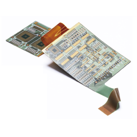
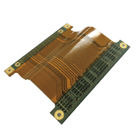
Printed Circuit Board Manufacturing - Rigid-Flex Boards

Production is possible from 2 layers to 8 layers. Prototyping of rigid-flex PCBs is available with short lead times and low prices.

We can produce from 2 to 8 layers. When it comes to rigid-flex PCBs, it often requires creating molds, which can be very expensive even for prototypes, and the production time can be significantly long. At K2 Corporation, we combine our experience as a rigid PCB manufacturer with our experience as a flexible PCB manufacturer to offer quick turnaround and low-cost prototypes of rigid-flex PCBs. We can flexibly accommodate complex shapes and special layer configurations, so please feel free to consult with us. For more details, please contact us or refer to our catalog.

  • Printed Circuit Board
  • substrate

ブックマークに追加いたしました

ブックマーク一覧

ブックマークを削除いたしました

ブックマーク一覧

これ以上ブックマークできません

会員登録すると、ブックマークできる件数が増えて、ラベルをつけて整理することもできます

無料会員登録

Special printed circuit board manufacturing IVH boards

A substrate that connects only the necessary layers without penetrating the holes in a multilayer substrate.

This is a substrate that connects only the necessary layers without penetrating the holes in a multilayer board. As the number of layers in printed circuit boards has increased, the demand for this has also grown. It can be manufactured using either blind via holes that connect the outer layers to the inner layers or inner vias that embed through holes in the inner layers. Additionally, it is compatible not only with standard multilayer boards but also with multilayer flexible boards and rigid-flex boards. For more details, please contact us or refer to the catalog.

  • Printed Circuit Board
  • substrate

ブックマークに追加いたしました

ブックマーク一覧

ブックマークを削除いたしました

ブックマーク一覧

これ以上ブックマークできません

会員登録すると、ブックマークできる件数が増えて、ラベルをつけて整理することもできます

無料会員登録

New Comprehensive Catalog from a Specialized Substrate Manufacturer 【*Low-Cost Solutions for Special Substrates!】

A comprehensive catalog full of hints for achieving ultra-short delivery times for special substrates is available for free!

At K2, we have all the manufacturing equipment necessary for circuit board production fully in-house, and by operating that equipment at 100%, we achieve shorter lead times and lower costs for special circuit boards and medium-lot products that are difficult for prototype manufacturers to handle. 1. They do not accommodate ultra-short lead times... 2. The initial costs for flexible boards are too high... 3. I was turned away when consulting about special circuit board manufacturing... 4. They do not accommodate short lead times for medium-lot production... 5. There are concerns about the quality of the circuit boards... We will solve these five issues faced by the circuit board manufacturing industry using our unique know-how. 【Case Studies】 ■ Resin filling (Pad on Via hole) specification ⇒ Where outsourcing would typically require an extra 3 days, we can handle it in 1 day! ■ Double-sided flexible circuit boards ⇒ Achieved shorter lead times and reduced initial costs by using laser processing instead of molds for shape processing! ■ 4-layer rigid-flex circuit boards (without reinforcement plates) ⇒ Normally 7 days, expedited response in 6 days! *For more details, please contact us or download our catalog to view.

  • Printed Circuit Board
  • substrate

ブックマークに追加いたしました

ブックマーク一覧

ブックマークを削除いたしました

ブックマーク一覧

これ以上ブックマークできません

会員登録すると、ブックマークできる件数が増えて、ラベルをつけて整理することもできます

無料会員登録

Latest Catalog of a Substrate Specialty Manufacturer

First, please consult with us! We offer low-cost and quick turnaround for special substrates such as rigid boards and flexible boards.

K2 has all the manufacturing equipment necessary for circuit board production fully equipped in-house, achieving 100% operation to realize shorter delivery times and lower costs for special circuit boards and medium-lot products that are difficult for prototype manufacturers to handle. 1. They don't respond to ultra-short delivery times... 2. The initial costs for flexible boards are too high... 3. I was turned down when consulting about special circuit board manufacturing... 4. They don't respond to short delivery times for medium-lot production... 5. I have concerns about the quality of the circuit boards... We solve five issues faced by the circuit board manufacturing industry with our unique know-how. *Currently offering free samples of special circuit boards to a limited number of 10 companies! For more details, please download the catalog from the form below or contact us.* [Case Studies] ■ Double-sided flexible circuit board ⇒ Achieved shorter delivery times and reduced initial costs by using laser processing instead of molds for shape processing! ■ 4-layer rigid-flex circuit board (without reinforcement plate) ⇒ Normally 7 days, express response in 6 days!

  • Printed Circuit Board
  • substrate

ブックマークに追加いたしました

ブックマーク一覧

ブックマークを削除いたしました

ブックマーク一覧

これ以上ブックマークできません

会員登録すると、ブックマークできる件数が増えて、ラベルをつけて整理することもできます

無料会員登録

Shortest 0.5 days! Ultra-short delivery for rigid PCBs [*Free samples available!]

In-house integrated production including gold plating line and ultra-short delivery response through operation every Saturday!

K2 offers high quality, low cost, and the ability to respond to ultra-short delivery times. The reason for this is that we have all the manufacturing equipment necessary for circuit board production fully equipped in-house and operating at 100%. We also have in-house facilities for copper and gold plating lines, which are often outsourced. Additionally, we are open on Saturdays to accommodate weekend orders. We will ensure thorough circuit board production while other companies are closed. *We are currently offering free circuit board samples through a lottery! [Problems We Can Solve] 1. They don’t respond to ultra-short delivery times… 2. The initial costs for flexible boards are too high… 3. I was turned away when consulting about special circuit board manufacturing… 4. They don’t respond to short delivery times for medium lot production… 5. I have concerns about the quality of the circuit boards… If you are facing any of these issues, please download our catalog or contact us.

  • Printed Circuit Board
  • substrate

ブックマークに追加いたしました

ブックマーク一覧

ブックマークを削除いたしました

ブックマーク一覧

これ以上ブックマークできません

会員登録すると、ブックマークできる件数が増えて、ラベルをつけて整理することもできます

無料会員登録