Printed circuit board
We deliver from prototypes to mass-produced products in a short lead time. Please feel free to consult us about anything related to circuit boards.
Each manufacturing process is carried out with thorough quality control by skilled workers. We produce single-sided boards, multilayer boards, flexible boards, aluminum boards, edge-through-hole boards, thin boards, build-up boards, BGA boards, wire bonding boards, and white LED boards.
- Company:トーヤ
- Price:Other


![[Introduction to Fair Process] Mechanism/Circuit Board Pattern Design](https://image.mono.ipros.com/public/product/image/ec4/2000822069/IPROS01198801785659023133.png?w=280&h=280)


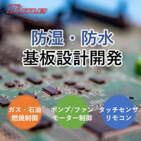
![Control board "Gas Combustion Equipment Control" [Safe Combustion - Zero Accidents]](https://image.mono.ipros.com/public/product/image/530/2000560391/IPROS21993140401657012384.jpeg?w=280&h=280)